RVN! 26 Banner revised (800 x 100 px) (600 x 100 px)

Universal Flash Storage: Webinar

Universal Flash Storage: Webinar
by Paul McLellan on 02-24-2012 at 2:24 pm

There has been a general trend for over a decade now towards the use of very fast serial interfaces instead of wide parallel interfaces. This has been driven by a number of different factors ranging from the lack of pins on an SoC, the difficulty of keeping wide parallel interfaces free of skew, limitations on printed circuit board wiring space and so on. Apart from the difficulty of building very fast serial interfaces, almost everything is upside.

JEDEC and MIPI (the Mobile Industry Processor Interface) were both working on high-performance serial I/O standards for data transfers between portable consumer devices. In 2010 these efforts were merged to create the Universal Flash Storage (UFS) standard. UFS is designed to offer a fast, reliable and simple means of supporting storage requirements in portable applications such as smart phones. It supports both embedded and removable card applications. Since it is intended primarily for portable applications, the standard features low power consumption.


Next week Arasan is having two live seminars on UFS and the Arasan UFS solution:

  • UniPro controller
  • M-PHY interface block
  • UFS block
  • UFS and UniPro drivers
  • Software stack
  • Hardware verification IP
  • Hardware validation platform

The live webinar will be on February 28th at 6pm PST (and a useful time for people attending in Asia) and again the next morning February 29th at 10AM PST. Register HERE.


Synopsys at DVCon: tutorial, lunch, keynote, exhibits and more

Synopsys at DVCon: tutorial, lunch, keynote, exhibits and more
by Paul McLellan on 02-24-2012 at 1:10 pm

DVCon is next week, which I’m sure you know already if you are in verification. Of course Synopsys has a rich product portfolio in verification and verification IP (VIP) so is pretty visible at the show.

On Wednesday they are sponsoring lunch. Several Synopsys customers will talk about their view of how the verification landscape is changing. Lunch will be in the Pine/Cedar ballroom from 12.30 onwards. No need to register specially if you are attending DVCon.

Following the lunch, Aart de Geuss, CEO of Synopsys will give the DVCon keynote Systemic Collaboration: Principles for Success in IC Design which looks at the big picture view of how the combination of technology and economics drives everything.

On Thursday, from 1.30 to 3.30 there is a Synopsys tutorial New Levels of Verification IP Productivity for SoC Verification. You need to register here for this if you want to attend. The tutorial is fairly technical and is focused on tnew features added to VIP and how to enable VIP in different environments. There is a demo of debugging at the protocol level (that is, at a much higher level than the actual signals and registers).

Of course Synopsys has a booth in the exhibit hall, number 1105. Exhibits are open 3.30 to 6.30 on Tuesday and 4.30 to 7.00 on Wednesday. You can register for just the exhibits for free.

The main DVCon website is here.

Oh, and while I’m here, Monday evening I’m moderating a panel session Hardware/Software Co-Design from a Software Perspective. All the details are in my earlier blog on the subject here.


Call for Papers: International Gathering for Application Developers!

Call for Papers: International Gathering for Application Developers!
by Daniel Nenni on 02-22-2012 at 8:40 pm

SemiWiki would like to call you, your co-workers, and your company to participate at ERSA Conference in Las Vegas , July 16-19, 2012. I will be there and it would be a pleasure to work with you on this very important event!

ERSA, is Engineering of Reconfigurable Systems and Algorithms. Since this year, the emphasis will be on the commercial and industrial challenges. We will have application developers’ session with many hot topics and featured sections. The aim is to connect researchers and developers, entrepreneurs; as well as developed countries with emerging markets. The industrial content of ERSA is not strictly reconfigurable computing.

The Hot Topic: “Reconfigurable Computing Application Development for Heterogeneous Run-time Environments”. Focus on challenges, tools, available technologies and opportunities when it comes to developing and supporting applications, both academic and commercial, that involve reconfigurable computing technologies across mobile, embedded, and HPC domains.

Featured sections:

“Hardware security and trust in reconfigurable heterogeneous systems”

“Developing IP cores and scalable libraries for heterogeneous systems”

You can arrange a demo, exhibition, seminar, tutorial, etc. Note there are over 2000 attendees together (ERSA is a part of Worldcomp). There are around 400 attendees with strong hardware design background. Thus, there is a high visibility of your company.

Note also that early advertisinghelps people to plan their travel to visit your presentation.

For more details, please visit ERSA website at http://ersaconf.org/ersa12 .

If you might be interested, please contactl: org@ersaconf.org , to discuss further details.

ERSA conference is also available as a Thread at SemiWiki:
http://www.semiwiki.com/forum/f2/international-conference-engineering-reconfigurable-systems-algorithms-1201.html, you can add comments there.

SemiWiki Blog:
http://www.semiwiki.com/forum/content/996-premier-international-gathering-%85-application-developers-ersa.html, forward to colleagues.


Seminar on IC Yield Optimization at DATE on March 14th

Seminar on IC Yield Optimization at DATE on March 14th
by Daniel Payne on 02-22-2012 at 3:59 pm

My first chip design at Intel was a DRAM and we had a 5% yield problem caused by electromigration issues, yes, you can have EM issues even with 6um NMOS technology. We had lots of questions but precious few answers on how to pinpoint and eliminate the source of yield loss. Fortunately, with the next generation of DRAM quickly introduced this yield issue was less urgent.
Continue reading “Seminar on IC Yield Optimization at DATE on March 14th”


Computer Architecture and the Wall

Computer Architecture and the Wall
by Paul McLellan on 02-22-2012 at 1:08 pm

There is a new edition of Hennessy and Patterson’s book Computer Architecture: A Quantative Approach out. The 5th edition.

There is lots of fascinating stuff in it but what is especially interesting to those of us who are not actually computer architects, is the big picture stuff about what they choose to cover. Previous editions of the book have emphasized different things, depending on what the issues of the day were (RISC vs CISC in the first edition, for example). The more recent editions have mostly focused on instruction-level parallelism, namely how do we wring more performance from our microprocessor while keeping binary compatibility. I was at the Microprocessor Design Forum years ago and a famous computer architect, I forget who, said that all of the work on computer architecture over the years (long pipelines, out of order execution, branch prediction etc) had sped up microprocessors by 6X (Hennesy and Patterson reckon 7X in the latest edition of their book). All the remaining 1,000,000X improvement had come from Moore’s law.

If there are a few themes in the latest edition they are:

  • How to do computation using the least amount of energy possible (battery life for your iPad, electricity and cooling costs for your warehose scale cloud computing installation)?
  • How can we make use of very large numbers of cores efficiently?
  • How can we structure systems to use memory efficiently?

The energy problem is acute for SoC design because without some breakthroughs we are going to run head on into the problem of dark silicon: we can design more stuff, especially multicore processors, onto a chip than we can power up at the same time. It used to be that power was free and transistors were expensive but now transistors are free and power is expensive. It is easy to put more transistors on a chip than we can power on.

The next problem is that instruction level parallelism has pretty much reached the limit. In the 5th edition it is relegated to a single chapter as opposed to being the focus of the book in the 4th edition. We have parallelism at the multicore SoC level (e.g. iPhone) and at the cloud computing (e.g. Google’s 100,000 processor datacenters). But for most stuff we simply don’t know how to exploit the architecture. Above 4 cores most algorithms see no speedup if you add more, and in many cases actually slow down, running more slowly on 16 cores than on 1 or 2.

Another old piece of conventional wisdom (just read anything about digital signal processing) is that multiplies are expensive and memory access is cheap. But a modern Intel microprocessor does a floating point multiply in 4 clock cycles but takes 200 to access DRAM.

These 3 walls, the power wall, the ILP wall, and the memory wall means that whereas CPU performance used to double every year and a half it is now getting to be over 5 years. How to solve this problem is getting harder too. Chips are too expensive for people to build new architectures in hardware. Compilers used to be thought of as more flexible than the microprocessor architecture but now it takes a decade for new ideas in compilers to get into production code, whereas the microprocessor running the code will go through 4 or 5 iterations in that time. So there is a crisis of sorts because we don’t know how to program the types of microprocessors that we know how to design and operate. We live in interesting times.


3D-IC Physical Design

3D-IC Physical Design
by Pawan Fangaria on 02-22-2012 at 10:00 am

When process nodes reached 28 nm and below, it appeared that design density is reaching a saturation point, hitting the limits of Moore’s law. I was of the opinion that the future of microelectronic physical design was limited to 20 and 14 nm being addressed by technological advances such as FinFETs, double patterning, HKMG (High-k Metal Gate) etc… Probably, this limitation pushed the industry to look at other avenues such as growing vertically giving rise to 3D-IC, also enabling SoC arena, which is of interest today.

Although the concept of 3D-IC is borrowed from 3D packaging, in the IC world it is definitely an important innovation which unfolds opportunities to go beyond Moore’s law with improved performance and power. Last October, Xilinx announced Virtex-7 2000T which is a 2.5D assembly using silicon interposer and metal interconnect through it to connect four FPGA dies on a single plane; further pushing the industry to actual 3D stacked dies, where multiple dies can be stacked one above the other in different configurations (B2F, F2F, B2B).


3D-IC advantages are aplenty (low power, large memory b/w, high density, high speed etc.) provided the associated challenges (Thermal, EMI, Power management, mechanical stress etc.) are handled well for reliability and planning is done well at the system level. When we talk of 3D, it is like planning for the whole house (all floors) where provisions for interior design have to be considered. Of course there are other challenges like parasitic extraction of TSVs (Through Silicon VIAs) and silicon interposers, physical verification of all dies together with their interconnections and DFT. In this article I am talking about physical design of 3D-IC which needs to be done meticulously to get the optimum result. Following are the steps –

Architecture exploration – This pertains to correct assembly, which needs to be done at the system level where specific die assignment can be done for Analog, Digital, memory, cache and computational modules of a microprocessor. Top level estimation has to be done at this level for optimum assignment to get the best power, speed and density.

Floorplanning – is at the heart of 3D-IC; partitioning at multiple planes including die orientation, TSV placement, keep outs from TSVs (Stress due to TSV can affect threshold voltage of a transistor near it), micro-bumps etc. need to be planned well. For Analog Digital mixed-signal design, proper hand-shake between the two needs to be planned. Thermal effects need to be taken care of and heat sinks need to be planned.

Placement – needs to consider breaking critical paths by adding TSV and using 2[SUP]nd[/SUP] plane to place part of the components. Further, VIAs should be minimized. RF and digital circuitry can be placed separately. TSV placement and micro-bump alignment need to be done.

Routing – needs to consider routing at each plane including backside Redistribution Layers (RDL) and wires connecting through TSVs.

Layout Editing – It goes without mention that editing support for TSVs for all types of interconnections – signal, PG and thermal, micro-bumps and the like is need to be provided. 3D viewing of layout has to be there.

While each tool needs to be extended to 3D capabilities, it also needs to adhere to standards to maintain reliability and interoperability. As the components of a 3D-IC can come from multiple vendors, it is essential that standards need to be defined and adhered for everyone to follow. Although we are late on standards, Standard Development Organizations (3DIC-Alliance, IEEE, JEDEC, SEMI, SI2) are working towards defining these. Exchange Formats for Thermal, Power Delivery Network, Mechanical Stress, Partitioning and Floorplanning and DFT are in the making. Until then, EDA tools in development need to be extensible such that they can adopt the standards later. JEDEC has already released Wide I/O Standard for 3D Memory which was needed since long. It also standardizes for boundary scan test, DRAM test and thermal sensor locations for reliability or memory operations.

3D-IC testing is a large challenge in itself requiring tests at wafer and TSV level in addition to chip level. The industry needs robust test standards to justify the investment in 3D-IC design and manufacturing. We can discuss this separately later.

By Pawan Kumar Fangaria
EDA/Semiconductor professional and Business consultant
Email:Pawan_fangaria@yahoo.com


Don’t go to Mobile World Congress without “MIPI IP Forecast 2011-2016”!

Don’t go to Mobile World Congress without “MIPI IP Forecast 2011-2016”!
by Eric Esteve on 02-22-2012 at 9:48 am

And if, like me, you don’t go to MWC, that’s the right time to get your version of the MIPI IP survey, the 3[SUP]rd[/SUP] version since the first launch in 2010, because IPNEST will give you a good reason to buy it during MWC: you will get it at a lower price. That will apply now and during the event, but only from today, and up to the 3[SUP]rd[/SUP] of March… But let’s have a look at the latest status about MIPI. MIPI is hot, MIPI is coming to the mainstream, don’t miss it!

MIPI follows the trends in the Electronic industry: the massive move from parallel to serial interconnect, as illustrated by PCI Express replacing PCI, SATA replacing PATA, HDMI or DisplayPort replacing LVDS based interconnect to Display material (computer screen or HDTV) etc… Using similar technologies in Mobile Devices is a natural move, but a specific attention has been taken to power consumption. MIPI has been specifically designed for portable electronic devices, battery powered, and lowering the power consumption is a key feature.

MIPI’s defined charter focusing on mobile platforms defines the markets addressed by the standards and the target products for those standards. That market is mobile handsets, from basic low-end, full-featured phones, to Smartphone. Since 2009, the MIPI alliance has decided to promote MIPI use in every kind of mobile Application, like Mobile Internet Devices (MID) and Media Tablet in the PC segment, or Handheld game console, Digital still camera and potentially all portable system in the Consumer Electronic segment.

In this survey, we have started to look at the MIPI use in the Mobile Handset segment and first derive a forecast in term of Integrated Circuits (IC) because we think that the more widely MIPI will be used in chips in production, the more stable and easier to manage the protocol will be. When more IC is in production means more efficient –and cheaper- test program, leading to a null or marginal impact on yield. More identical IC in production also means cheaper production cost and consequently a lower Average Selling Price (ASP).

Such a virtuous cycle is expected to lead to a wider adoption for MIPI technology. When MIPI was introduced and started to be used in the high end of the wireless handset segment, most of the early adopters had both the knowhow and the resource needed to develop the solution internally (or enough money to use design service) instead of sourcing MIPI externally as a standard IP. They probably also prefer at that time not to depend to external sourcing for a function to be integrated into strategic IC like Application Processor, or Camera Controller whatever is their core business. This was the first phase for MIPI, being considered as an emerging technology, which also means more expansive to integrate, and more risky.

With the success of this first phase, illustrated by the number of MIPI powered IC in production passing the one billion range (in 2011 according with our forecast) will come the second phase, in 2012-2013, where MIPI will be integrated in the majority of the smartphone segment, some of the featured phone and being considered in design starts serving other segments than the wireless handset segment. This second phase will lead to several consequences: the early adopters may start to use externally sourced MIPI functions (MIPI is no more a strategic differentiator) instead of internal design; the many followers, attracted by the very high volumes in the wireless handset industry, many of them in China or Taiwan, will certainly decide to “buy” instead of “make” MIPI function, for TTM or knowhow related reasons; the chip makers developing IC to serve other market segment will also prefer to buy, for the same reasons.

All of them selecting the technology to get full benefit, on top of the low power consumption, from MIPI usage:

  • Standardized Interconnect protocol: an OEM can run seamless integration in the system of the different IC, providing they comply with the same MIPI Interfaces.
  • Interchange suppliers at low risk: an OEM can easily move from one IC supplier to another for the same function (for example a camera controller IC), at least at the Interface level
  • There are different specifications for the Controller (CSI, DSI, LLI and so on), but only two for the PHY (D-PHY and M-PHY): many specifications, but an easier learning curve to physically interface the application processor with Camera, Display, Modem, Mass Storage, WLAN, Remote Coprocessor…!

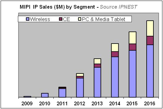
We expect this second phase to lead to high growth sales of MIPI IP; we propose a forecast for the IP licenses sales for the 2010-2016 periods, including “actual” results from IP vendors whenever it’s possible.

We have also proposed a review of the different IP vendors actively marketing MIPI PHY IP, or Controller IP or both. This competitive analysis could benefit to:

  • MIPI new adopters, or the chip makers integrating MIPI in devices serving wireless handset segment (smartphone or not), Media Tablet and PC and Consumer Electronic segments,
  • IP vendors, who desire to develop a new IP business or consolidating existing business and invest resources on line with MIPI IP business potential.
  • VIP vendors who invest into this new source of business, after having supported USB, SATA, PCI Express…

This MIPI IP survey or one of the two previous versions has been sold to IP vendors (already supporting MIPI or in the decision process to support these specifications), VIP vendor and chip makers. This report is unique: it’s the only one where the reader can find both an IC and an IP forecast for MIPI, as well as a competitive analysis of the IP –and VIP- vendors. As such, if your company is or will be involved into MIPI, you need to have it.

Eric Esteve from IPNEST– Table of Content for “MIPI IP Forecast 2011-2016” available here


Custom Processors: Webinar

Custom Processors: Webinar
by Paul McLellan on 02-21-2012 at 5:24 pm

What is a custom processor? Or Application Specific Instruction-set Processor (ASIP) which is the buzzword which may or may not catch on.

Most programming is done on a processor with a fixed instruction set: think Intel x86 or ARM. Intel or ARM decided on what instructions to include, based on a lot of benchmarking across a wide range of different types of workloads. So there is a sense in which these are lowest common denominator instruction sets. This is clearly a good approach for the microprocessor in your cell-phone or your laptop because they have to run a wide range of workloads too. But if you are designing a processor for a specific application domain, such as decoding MPEG video, then the general solution may be very far from optimal, especially in performance or power or both. Since a major reason to create a special purpose processor is to offload a general purpose processor, then you really need to hit a much better performance/power point to justify the effort. Otherwise why bother?

Synopsys didn’t used to be in the processor business, but they acquired the ARC processor with the Virage acquisition and a flavor of the Lisa processor generator with the CoWare acquisition. There is a lot of technology in a custom processor. So much that you can’t really do it by hand. RTL alone is not enough. After all, a processor is no use without assemblers, linkers, compilers, debuggers. You probably want an Instruction Set Simulator (ISS), a very fast model, so you can develop code in parallel with the initial implementation of the chip containing your processor. If you did this by hand, apart from being too expensive, you wouldn’t have a lot of confidence that the instruction set in the processor matched the ISS and matched the compiler and so on. So the only way to have an ASIP is to have an ASIP generator that starts from a specification of the processor and generates all the other views automatically.

Synopsys has a webinar coming up next week on this topic. It is next Tuesday, February 28th, at 8am (Pacific). The webinar is presented by Drew Taussig, who came to Synopsys by way of CoWare where he was part of the processor designer product team. So he’s been dealing with this area for a long time.

Register here.


Will the last 8051 please turn out the lights?

Will the last 8051 please turn out the lights?
by Don Dingee on 02-21-2012 at 2:38 pm

The words no engineer or supply chain professional wants to hear: end-of-life. It’s a reality of the semiconductor business, however – even the cheapest parts reach the point, eventually, where producing and selling them becomes inefficient. Is it reasonable that a microcontroller architecture outlive the people who designed it in? Continue reading “Will the last 8051 please turn out the lights?”