
When a company develops chip for the military industry, I would prefer these chips to be using a 100% reliable technology. I am sure that you too! For certain application, 99%, or even 99.99% rate of confidence is not enough. Would you accept to fly in an airplane if you still have 1 out of 10,000 chances to crash? Would you accept living in an area which could be destroyed by one of this very “efficient” atomic bomb, even knowing at 99.99% that it shouldn’t happen?

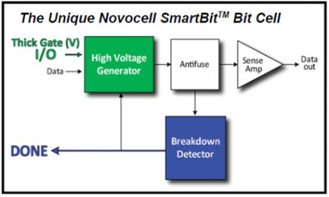
That’s why it’s good to hear that a “United States military contractor has decided to adopt the 100% reliable Smartbit™-based non-volatile memory (NVM), a one-time programmable (OTP) antifuse product from Novocell, taped out in a 32nm SOI process at IBM’s foundry”. All Novocell Smartbit-based NVM IPproducts avoid the limitations of traditional embedded NVM technology by utilizing the patented design and dynamic programming and monitoring process of the Novocell Smartbit bit cell, ensuring that 100% of customers’ embedded bit cells are fully programmed. The result is Novocell’s unmatched 100% yield and unparalleled reliability, guaranteeing customers that their data is fully programmed initially, and will remain so for an industry-leading 30 years or more. We have explained in Semiwiki the mechanisms allowing Novocell to claim this 100% reliability: “breakdown detector” circuitry, checking that hard breakdown as effectively occurred.
The point to be highlighted is that Smartbit technology has been ported on chips based on IBM’s 32nm, Silicon-on-Insulator (SOI) technology, which was jointly developed with GLOBALFOUNDRIES and other members of IBM’s Process Development Alliance, with early research at the University at Albany’s College of Nanoscale Science and Engineering. The technology vastly improves microprocessor performance in multi-core designs and speeds the movement of graphics in gaming, networking, and other image intensive, multi-media applications. The SOI process was used to build the microprocessor that powered IBM Watson, the question-answering computer that won the Jeopardy! quiz show in early 2011.

When I look back at my very first job in SC industry, it was with Philips Research Lab (LEP), trying to identify and characterize EL2 traps in GaAs substrate by measuring current flow within a handmade diode (I remember I had to hard wire the diode using a golden wire soldered under a microscope!…FYI, the picture is of the very first integrated circuit handmade by Jack Kilby).
When I asked my manager why Philips was spending so much money on GaAs although Silicon was much easier to process, the answer was: because the electron mobility was higher by a factor of five (I already knew it from University), allowing running the devices at higher frequency, AND because GaAs substrate is nonconductor, or, if you prefer insolent. What are the benefits? At first, no leakage current in the substrate, this part of the power consumption which tend to be higher when the technology node decrease. We can see today with the latest technologies (28 or 20 nm) that the power dissipation tends to stay flat instead of decreasing, due to this effect.
The second benefit, I could really appreciate it when doing my PhD later on, studying the parasitic resistor and capacitor on CMOS (Silicon) technology: the delay in any interconnects wire can be simply modeled as an RC delay. To change the resistivity value (the R) you can change the wire material, but the capacitor value is directly linked with the substrate conductivity: it will be much lower if the substrate is insolent. At the time I was measuring and modeling this effect, the delay lost in interconnects was about a few % of the gate delay. The impact of the delay spent in interconnects has dramatically increased in proportion: the technology feature size has decreased by a factor of 100 (2um to 20nm), so approximately the gate delay, when the interconnect delay tend to stay flat. Thus, the proportion has passed from a few % to a few times! If you could suppressed or strongly decrease the capacitance (the “C” in the RC), you could better benefit from the technology downscaling (Moore’ law).
As a matter of fact, Philips Research Lab could never successfully create a GaAs oxide (like SiO2, easy to create for the Silicon), thus the GaAs usage to build Large Scale of Integration (LSI) device was not practically possible, and the technology has only been used to process discrete devices, but unfortunately not to process SoC. If you want to build a SoC and benefit from an insolent substrate, the Silicon On Insulator (SOI) technology is the only route today. But, if you want the technology to be successful, you need to benefit from an IP Ecosystem as large as possible, and Smartbit is one piece of this Ecosystem.
Eric Esteve from IPNEST –
Share this post via:


TSMC CoWoS versus Intel EMIB Semiconductor Packaging