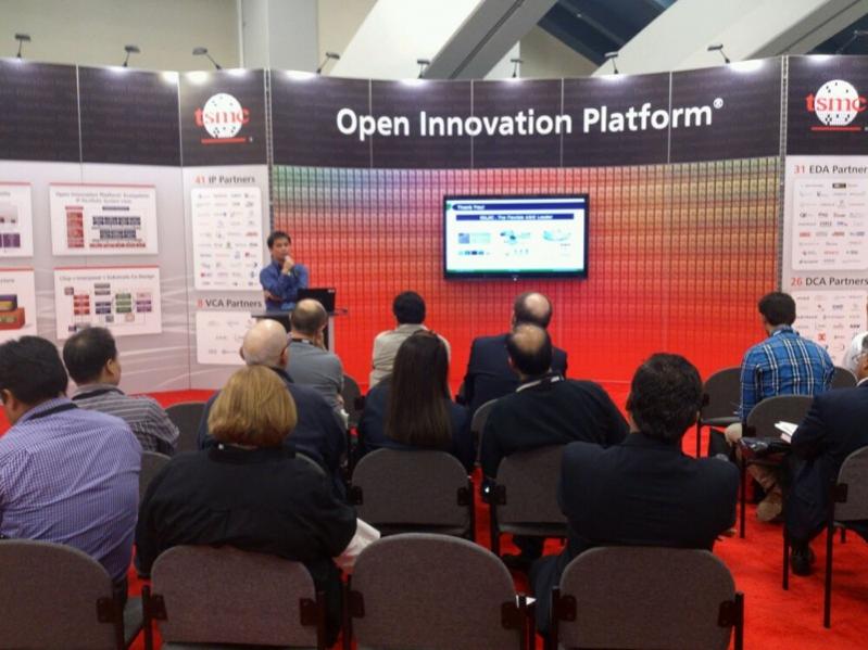
 One of the truisms of today’s disaggregated semiconductor design and manufacturing model is counter-intuitive to the do-it-yourself focus that is at the heart of every engineer. And yet, time and time again, success rewards those who understand that with today’s ever increasing complexity, it is difficult, if not impossible, to be all semiconductor things to all people.
This lesson was reinforced during a presentation at DAC 2012 from Global Unichip that focused on the services bundled into their Flexible ASIC Model[SUP]TM[/SUP] that allows semiconductor designers to focus on their core competency. What impresses me about their approach, is that GUC doesn’t insist on a hard-and-fast hand off point, but rather provides the flexibility for each company to determine where their core competency begins and ends.
GUC’s business today is being driven by high gate count, advanced technology, and low power SoC designs. Low Power is definitely key to much of today’s innovation. GUC’s low power design services start with defining specific low power library and power gating techniques. It also encompasses DVFS and AVFS services along with low power verification. But the heart of their design services lies in their low power competency, their domain IP integration and their highly sophisticated design for test (DFT).
The GUC Low Power Competency goes under the brand name PowerMagic® and covers IP that provide both internal and external power shutdown that has been proven on more than 80 designs over the past five years. Dynamic power is a big concern for low power, high performance designs. Working through different methodologies GUC has mastered the ability to efficiently perform clock gating at the architecture level. They are also experts at designing for multiple supply voltages on a single chip and dynamic voltage frequency scaling. The key to their success is the ability to design-in changes to the supply voltage and frequency based on the current processor loading.
Another design variable that drives both design quality and time-to-market success is the ability to integrate high speed interface IP into low power designs at both the chip and system level. To that end, GUC began developing and designing its own high speed interface IP, including SerDes, PCI Express 3.0, USB 3.0, DDR2/3, LPDDR2/3 and a number of others starting at 65nm. Today, that high speed interface IP portfolio covers production nodes down to 28nm and continues to shrink to 20nm. Another GUC service is customizing IP for each application to meet required specification. To achieve comprehensive domain IP integration, package influences also need to be taken into consideration.
In parallel, GUC extends its high speed design capabilities through its Design for Test (DFT) services. The key objective is to improve yield by reducing peak power during testing so as to cut down the cost of testing.
While there is much more to the GUC low-power methodology than I can blog here, the point is that low power at high performance is a difficult design challenge, one that vexes many designers and requires a new found expertise. The bottom line is that it might be worth checking out silicon proven low power designs specialists the next time you face that specific challenge.


Musk’s Orbital Compute Vision: TERAFAB and the End of the Terrestrial Data Center