You are currently viewing SemiWiki as a guest which gives you limited access to the site. To view blog comments and experience other SemiWiki features you must be a registered member. Registration is fast, simple, and absolutely free so please,
join our community today!
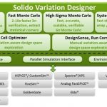
With the insatiable wafer appetites of the fabless semiconductor companies in the mobile space, yield has never been more critical. The result being better EDA tools every year and this blog highlights one of the many examples. It has been a pleasure writing about Solido Design Automation and seeing them succeed amongst the foundries… Read More
The existence of TSMC’s Open Innovation Platform (OIP) program further sped up disaggregation of the semiconductor supply chain. Partly, this was enabled by the existence of a healthy EDA industry and an increasingly healthy IP industry. As chip designs had grown more complex and entered the system-on-chip (SoC) era, the amount… Read More
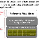
Today TSMC announced three reference flows that they have been working on along with various EDA vendors (and ARM and perhaps other IP suppliers). The three new flows are:
- 16FinFET Digital Reference Flow. Obviously this has full support for non-planar FinFET transistors including extraction, quantized pitch placement, low-vdd
…
Read More
I’ve written before about the basic capabilities of Sidense’s single transistor one-time programmable memory products (1T-OTP). Just to summarize, it is an anti-fuse device that works by permanently rupturing the gate oxide under the bit-cells storage transistor, something that is obviously irreversible.… Read More
At TSMC’s OIP on October 1st, Mentor Graphics have 5 different presentations. Collect the whole set!
11am, EDA track. Design Reliability with Calibre Smartfill and PERC. Muni Mohan of Broadcom and Jeff Wilson of Mentor. New methodologies were invented for 28nm for smart fill meeting DFM requirements (and at 20nm me may … Read More
Ecosystem is everything when it comes to modern semiconductor design, especially if it is mobile. The fabless semiconductor industry has been all about ecosystem since the beginning and that is why we hold supercomputers in our hands today, believe it. After the invention of the transistor in 1947, and the invention of the integrated… Read More
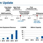
The history of TSMC and its Open Innovation Platform (OIP) is, like almost everything in semiconductors, driven by the economics of semiconductor manufacturing. Of course ICs started 50 years ago at Fairchild (very close to where Google is headquartered today, these things go in circles). The planarization approach, whereby… Read More
It now appears that Steve Ballmer was suddenly given his walking papers at the urging of an activist investor (ValueAct) and with the concurrence of Bill Gates. Wall Street’s growing impatience tends to coincide when the Innovators Dilemma scenario has taken hold of a company that has been unable to overcome its challengers. Why… Read More
I attended the semi-annual SEMI Silicon Valley Lunch meeting last week. The semiconductor equipment people are the ones that really know what is going on. People can talk about capex numbers on conference calls but it is the equipment vendors who either do or do not get orders for particular types of equipment. In turn, the analysts… Read More
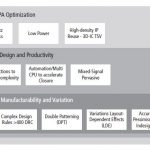
I think by now all of us know, or have heard about 20nm process node, its PPA (Power, Performance, Area) advantages and challenges (complexity of high design size and density, heterogeneity, variability, stress, lithography complexities, LDEs and so on). I’m not going to get into the details of these challenges, but will ponder… Read More