You are currently viewing SemiWiki as a guest which gives you limited access to the site. To view blog comments and experience other SemiWiki features you must be a registered member. Registration is fast, simple, and absolutely free so please,
join our community today!
Toshio Nakama is the founder and the CEO of S2C and also a strong advocate of FPGA accelerated ASIC/SoC design methodology. Mr. Nakama devotes much of his time in promoting scalable Prototyping/Emulation hardware architecture and defining automated software specifications. He first started his career at Altera in 1997 and … Read More
In 2016 SemiWiki published a book “Prototypical: The Emergence of FPGA-Based Prototyping for SoC Design”. Today we are writing Prototypical II since a LOT of prototyping innovation has happened in the last four years, absolutely.
For example:
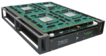
Quad 10M Prodigy™ Logic System extends the capacity leadership to simplify… Read More
FPGAs have been used for ASIC prototyping since the beginning of FPGAs (1980s) allowing hardware and software designers to work in harmony developing, testing, and optimizing their products. We covered the history of FPGAs in Chapter 3 of our book “Fabless: The Transformation of the Semiconductor Industry”, which includes … Read More
I haven’t sat down to speak with S2C since we collaborated on the book, PROTOTYPICAL, published just before DAC 2016 and even then, I hadn’t spoken to Toshio Nakama, their CEO. Toshio splits his time between the San Jose headquarters and the Shanghai headquarters so getting time to meet face-to-face has been challenging. I was finally… Read More
This interview originally appeared as the foreword to our book “Prototypical: The Emergence of FPGA-based Prototyping for SoC Design” but I thought it would be worth publishing for those of you who have not downloaded it yet. I also wanted to mention that our friends at S2C are currently offering a 50% discount on the… Read More
The health of the semiconductor industry revolves around the “start”. Chip design starts translate to wafer starts, and both support customer design wins and product shipments. Roadmaps develop for expanding product offerings, and capital expenditures flow in to add capacity enabling more chip designs and wafer starts. If… Read More
With major semiconductor mergers and acquisitions running rampant in 2015 (more than double the M&A activity in 2014), the question is where will we go from here? There are many different ways to slice this but for this blog let’s talk about the thousands of semiconductor professionals that will be changing jobs as a result … Read More
FPGA prototyping is beginning its move to the forefront of design and verification. More and more companies are turning to this technology not only for in-circuit testing and earlier software development but also for refining, validating, and implementing chip architecture. The increases in design size and complexity as well… Read More