You are currently viewing SemiWiki as a guest which gives you limited access to the site. To view blog comments and experience other SemiWiki features you must be a registered member. Registration is fast, simple, and absolutely free so please,
join our community today!
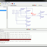
Spice view of a design, block or fragment of the design is probably the lowest level of functional description of a circuit in terms of transistors, resistors, capacitors, interconnect and so on, which in several ways acts as an ultimate proof of pudding for any semiconductor design before manufacturing. However, it’s generally… Read More
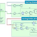
In a complex environment of semiconductor design where an SoC can have several millions of gates and multiple number of IPs at different levels of abstractions from different sources integrated together, it becomes really difficult to understand and debug the overall SoC design. Of course, along with the SoC integration, optimization… Read More
In a complex world of SoCs with multi-million gates and IPs from several heterogeneous sources, verification of a complete semiconductor design has become extremely difficult, and it’s not enough. In order to ascertain the right intent of the design throughout the design cycle, debugging at various stages of the design cycle… Read More
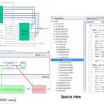
A very popular acronym is ‘WYSIWYG’ – What You See Is What You Get! This is very true and is important to visualize things to make it better in various aspects such as aesthetics, compactness, organization, structure, understandable for correction and so on; the most important, in case of semiconductor design, is being able to identify… Read More
When we talk about parasitic, we talk about post layout design further expanded in terms of electrical components such as resistances and capacitances. In the semiconductor design environment where multiple parts of a design from different sources are assembled together into highly complex, high density SoC, imagine how complex… Read More
In an environment of SoCs with tough targets of multiple functionalities, smallest size, lowest power and fastest performance to achieve within a limited design cycle window in order to meet the rigid time-to-market requirements, any day spent without success becomes very frustrating for a designer. Especially during tape-out… Read More