You are currently viewing SemiWiki as a guest which gives you limited access to the site. To view blog comments and experience other SemiWiki features you must be a registered member. Registration is fast, simple, and absolutely free so please,
join our community today!
Memory designers need to predict the timing, current and power of their designs with high accuracy before tape-out to ensure that all the design goals will be met. Extracting the parasitic values from the IC layout and then running circuit simulation is a trusted methodology however the accuracy of the results ultimately depend… Read More
Apple will purchase close to eightBILLION dollars in parts from Samsung for the iSeries of products this year alone, making Apple Samsung’s largest customer. Samsung is also Apple’s largest competitor and TSMC’s most viable competitive foundry threat so it was no surprise to see Apple and TSMC team up on the next generations of… Read More
Semiconductor manufacturing equipment shipments have leveled off after a strong rebound from the 2008-2009 downturn. August 2011 three-month-average shipments based on combined data from SEMI (North American and European companies) and SEAJ (Japanese companies) were $2.9 billion, down from a peak of $3.2 billion in May … Read More
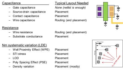
As analog and mixed-signal designers move to very advanced geometries, they must grapple with more and more complex considerations of the silicon. Not only do nanometer CMOS devices have limitations in terms of analog-relevant characteristics such gain and noise performance, but they also introduce new sources of variation… Read More
Fast Track Seminarsby Paul McLellan on 09-15-2011 at 6:11 pmCategories: EDA
Atrenta’s SoC realization seminars, “Fast Track Your SoC Design” have started.The first one was in Ottowa last Tuesday, and it was a full house. In a straw poll, most of the attendees acknowledged facing IP handoff and quality issues. The keynote speaker was Dr Yuejian Wu, director of ASIC development at Infinera… Read More
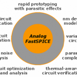
In working with TSMC and GlobalFoundries on AMS design reference flows I have experienced first hand the increasing verification challenges of nanometer analog, RF, and mixed-signal circuits. Tools in this area have to be both silicon accurate and blindingly fast! Berkeley Design Automation is one of the key vendors in this … Read More
Going up! Power and performance issues, along with manufacturing yield issues, limit how much bigger chips can get in two dimensions. That, and the fact that you can’t manufacture two different processes on the same wafer, mean that we are going up into the third dimension.
The simplest way is what is called package-in-package… Read More
I went to the second Global Technology Conference yesterday. It started with a keynote by Ajit Manocha who is the CEO of about 2 months. I hadn’t realized until someone asked him during the press lunch that he is technically only the “acting” CEO. Actually, given his experience he might be the right person anyway,… Read More
The economic news lately has been bleak. U.S. GDP grew at an anemic 0.4% in 1Q 2011 and 1.0% in 2Q 2011 – leading to increased concerns about a double-dip recession. High government debt levels in the U.S. and several European nations have contributed to volatile stock markets. The news does not seem to be any better for the semiconductor… Read More
Verifying circuits on advanced process nodes has always been difficult, and it’s no easier with today’s nanometer CMOS processes. There’s a great paradox in nanometer circuit design and verification. Designers achieve their greatest differentiation when they implement analog, mixed-signal, RF and custom … Read More