You are currently viewing SemiWiki as a guest which gives you limited access to the site. To view blog comments and experience other SemiWiki features you must be a registered member. Registration is fast, simple, and absolutely free so please,
join our community today!
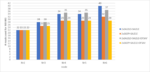
Earlier this month, TechInsights did a teardown of the Kirin 9030 chip found in Huawei’s Mate 80 Pro Max [1]. Two clear statements were made on the findings: (1) the transistor density of SMIC’s “N+3” process was definitely below that of the earlier 5nm processes from Samsung and TSMC, and (2) metal pitch was aggressively scaled
…
Read More
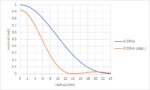
Previously, I had indicated how detrimental stochastic effects at pitches below 50 nm should lead to reconsidering the practical resolution limit for EUV lithography [1]. This is no exaggeration, as stochastic effects have been observed for 24 nm half-pitch several years ago [2,3]. This then leads to the question of whether … Read More
In recent advanced nodes, via and cut patterning have constituted a larger and larger portion of the overall BEOL mask count. The advent of SALELE [1,2] caused mask count to increase for EUV as well, resulting in costs no longer being competitive with DUV down to 3nm [3]. Further development by TEL [4] has shown the possibility for… Read More
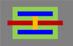
The point spread function is the basic metric defining the resolution of an optical system [1]. A focused spot will have a diameter defined by the Airy disk [2], which is itself a part of the diffraction pattern, based on a Bessel function of the 1st kind and 1st order J1(x), with x being a normalized coordinate defined by pi*radius/(0.5… Read More
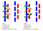
In this article, we will explore the use of self-aligned litho-etch-litho-etch (SALELE) double patterning for BEOL metal layers in the 7nm node (40 nm minimum metal pitch [1]) with DUV, and 5nm node (28 nm minimum metal pitch [2]) with EUV. First, we mention the evidence that this technique is being used; Xilinx [3] disclosed the… Read More