You are currently viewing SemiWiki as a guest which gives you limited access to the site. To view blog comments and experience other SemiWiki features you must be a registered member. Registration is fast, simple, and absolutely free so please,
join our community today!
Perhaps the most innovative and effective Extension implant does not involve an implant at all, but is instead an etch followed by a selective epitaxial deposition.
In this Extension fabrication methodology the Source/Drains regions in a planar device are etched away in the normal fashion to accommodate the replacement Source/Drain… Read More
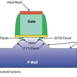
The problem of traditional FinFET Extension Implant doping concerns the awkward 3-dimensional structure of the fin. Because the Extension Implant defines the conductive electrical pathway between the Source/Drains and the undoped channel portion of the fin, it is essential that the fin be uniformly doped all three of its surfaces… Read More
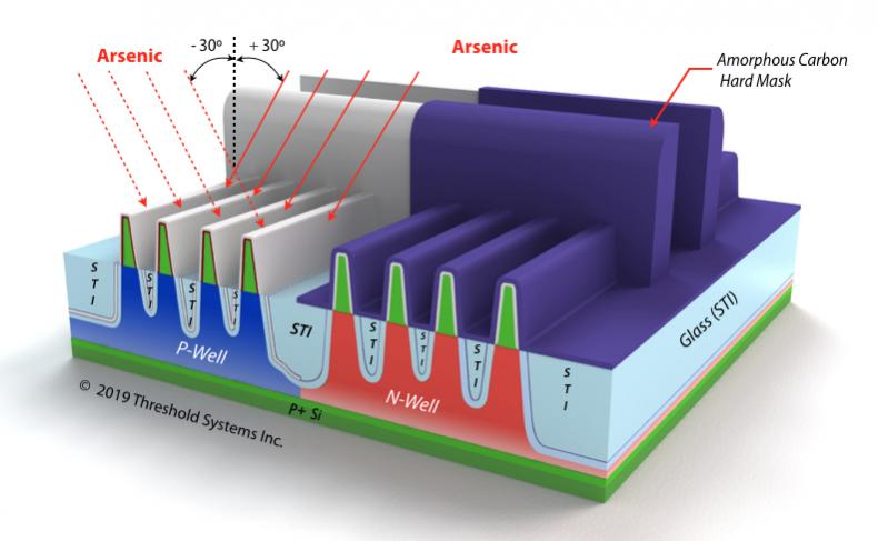
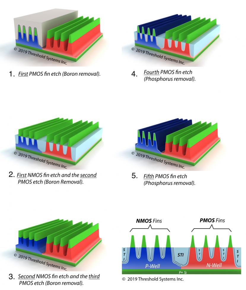
Like many others, we have often wondered why the PMOS fins on advanced microprocessors from Intel are narrower than the NMOS fins (6nm versus 8nm). This unusual dimensional difference first occurred at the 14nm node and it coincided with the introduction of Solid State Doping (SSD) of the fins at this node.
We have concluded that… Read More
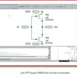
Simulation of Novel TFT Devicesby admin on 01-27-2014 at 5:45 pmCategories: EDA
Traditionally logic devices built on top of thin-film-transistors (TFTs) have used one type of device, either an NMOS a-Si: TFT (hydrogenated amorphous silicon) or a PMOS organic device. Recently a-Si:H and pentacene PMOS TFTs have been integrated into complementary logic structures similar to CMOS. This, in turn, creates… Read More