You are probably familiar with the acronym PPA, which stands for Power/Performance/Area. Sometimes it is PPAC, where C is for cost, since there is more to cost than just area. For example, did you know that adding an additional metal layer to a chip dramatically increases the cost, sometimes by millions of dollars? It requires a … Read More
Tag: paul mclellan
Worldwide Design IP Revenue Grew 12.4% in 2017
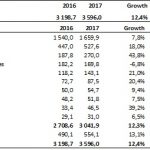
When starting SemiWiki we focused on three market segments: EDA, IP, and the Foundries. Founding SemiWiki bloggers Daniel Payne and Paul McLellan were popular EDA bloggers with their own sites and I blogged about the foundries so we were able to combine our blogs and hit the ground running. For IP I recruited Dr. Eric Esteve who had… Read More
Free Pivotal Semiconductor Books!
Just as a reminder, there are three semiconductor books in PDF format available for free on SemiWiki.com. The only hitch is that you must be a registered SemiWiki member to download them. If you are not currently a member please join here as my guest:… Read More
FREE Fabless: The Transformation of the Semiconductor Industry!
As most of you know SemiWiki published a book which is a really nice history of the fabless semiconductor ecosystem. Thousands of people have copies, we have received many compliments on it, and we are very proud. As a thank you to all SemiWiki members I would like to offer a free electronic version of the book (PDF). You can access it… Read More
Free Copy of EDAgraffiti!
Last month we offered a free PDF version of our book “Fabless: The Transformation of the Semiconductor Industry”, for the greater good. More than thirteen thousand people have downloaded it thus far so we would like to keep the momentum going with another book giveaway. Paul McLellan has graciously offered his book… Read More
Applying EDA Concepts Outside Chip Design
(I changed the title of this piece as an experiment) Paul McLellan recently wrote on the topic of new ventures crossing the chasm (getting from initial but bounded success to a proven scalable business). That got me to thinking about the EDA market in general. In some ways it has a similar problem, stuck at $5B or so and single-digit… Read More
The Best and Worst of #51DAC!
When people ask which DAC is the most memorable I used to say my first because I was a new college grad and it really was exciting. The next DAC was memorable since it was in Las Vegas and my beautiful wife joined me. This year was DAC number 30 for me and of course it will be the most memorable since I signed hundreds of copies of “Fabless: … Read More
Just Released! Fabless: The Transformation of the Semiconductor Industry
The book “Fabless: The Transformation of the Semiconductor Industry” is now available in the Kindle (mobi) and iBooks (ePub) formats. We are really looking forward to your feedback before we go to print in March. This was truly a Tom Sawyer experience for me. As the story goes Tom made whitewashing a fence seem like fun so his friends… Read More
SemiWiki Hits Major Readership Milestone!
For those of you who follow SemiWiki and the fabless semiconductor ecosystem it has been a very interesting two years:
The Semiconductor Wiki Project, the premier semiconductor collaboration site, is a growing online community of professionals involved with the semiconductor design and manufacturing ecosystem. Since going… Read More
Partitioning Panel
I moderated a panel on partitioning today and I have to say that I learned some things. The panelists were Jonathan DeMent from IBM, Santosh Santosh from NVIDIA and Hao Nham of eSilicon. Considering the different types of designs being done their approach to partitioning and the reasons for doing so were very similar.
When you first… Read More


