You are currently viewing SemiWiki as a guest which gives you limited access to the site. To view blog comments and experience other SemiWiki features you must be a registered member. Registration is fast, simple, and absolutely free so please,
join our community today!
China’s recent achievement of a 7nm-class foundry node using only DUV lithography [1] raises the question of how far DUV lithography can be extended by multipatterning. A recent publication at CSTIC 2023 indicates that Chinese groups are currently looking at extension of DUV-based multipatterning to 5nm, going so far… Read More
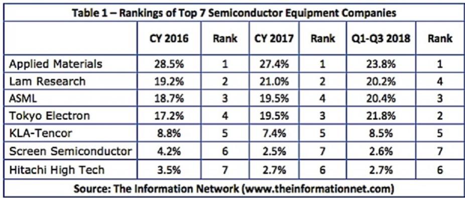
Semiconductor equipment vendor ranking, which didn’t change much between 2016 and 2017, is undergoing a makeover, as Lam Research, ASML, and Tokyo Electron (TEL) are switching places and top-ranked Applied Materials is getting closer to losing its number one ranking.
Since the 1990s, Applied Materials has been the market leader… Read More
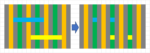
Place & route in the 16/14nm era requires a new approach since it is significantly more complex. Of course, every process generation is more complex than the one before and the designs are bigger. But modern processes have new problems. The two biggest changes are FinFETs and double patterning.
FinFETs, as I assume you know,… Read More
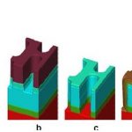
At major EDA events, CEDA (the IEEE council on EDA, I guess you already know what that bit stands for) hosts a lunch and presentation for attendees and others. This week was ICCAD and the speaker was Lars Liebmann of IBM on The Escalating Design Impact of Resolution-Challenged Lithography. Lars decided to give us a whirlwind tour … Read More
Engineers are always looking to improve the efficiency of how they work, but don’t want to sacrifice accuracy in the process. This is true in the world of semiconductor process development, where traditional build-and-test cycles are both time and resource intensive. But what if there was a way to do certain steps in a ‘virtual’… Read More