You are currently viewing SemiWiki as a guest which gives you limited access to the site. To view blog comments and experience other SemiWiki features you must be a registered member. Registration is fast, simple, and absolutely free so please,
join our community today!
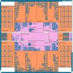
One area of iteration that is becoming more problematic is between floorplanning and synthesis. So much of timing is driven by placement that fixing timing and even power often involves not just re-synthesis and re-placement but alterations to the floorplan. The Achilles heel of existing methods is that floorplanning tools … Read More
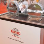
One of the highlights of the TSMC 2013 Open Innovation Platform® Forum was the Partner Award Ceremony. TSMC awarded Berkeley Design Automation (BDA) with the TSMC Open Innovation Platform’s Partner of the Year Award 2013 for joint development of 16nm FinFET design infrastructure. I talked with Ravi Subramanian, BDA CEO,… Read More
When new restaurants open they sometimes have what is called a ‘soft opening’ where they open a few days earlier than the official opening night. They are less busy since nobody knows they are open yet, maybe the whole menu isn’t available and expectations may be lower. Of course, Broadway productions also often… Read More
One of TSMC’s two big Silicon Valley events each year is the Open Innovation Platform (OIP) Forum. This year it is on Tuesday October 1st. It is in the San Jose Convention Center and starts at 9am (registration opens at 8am). Pre-registration to attend is now open here or click on the image to the right.
From 9.10 to 9.40 is the … Read More
You may say, “Why should I worry about synchronizer failures when I have never seen one fail in a product?” Perhaps you feel that the dual-rank synchronizer used by many designers makes your design safe. Furthermore, those chips that have occasional unexpected failures never show any forensic evidence of synchronizer failures.… Read More
Very rarely does the FPGA designer, especially with respect to RADAR, think of the FPGA as a floating point processor. Just to be sure I asked my 6 year old and she agreed. But you know what, the Xilinx FPGAs float. Go try it, order some up and fill up the tub.
Anyways I purpose a duel to the avid VHDL coder. I want you to design me a Sine(x) … Read More
Silvaco is the leading supplier of TCAD software, and a major supplier of EDA software for circuit simulation and design of analog, mixed-signal and RF integrated circuits.
The company was founded in 1984 by Dr. Ivan Pesic. The initial product, Utmost, quickly became the industry standard for parameter extraction, device characterization… Read More
As an Oakland Raider season ticket holder I attend as many Raider home games as possible. If you have ever attended a live sporting event at a large stadium, and you travelled by car, you are probably familiar with the traffic problems that occur at the end of the game when everyone wants to leave the stadium parking lot at the same time.… Read More
The first thing to realize about Dassault’s Simulation Lifecycle Management platform is that in the non-IC world where Dassault primarily operates, simulation doesn’t just mean functional verification or running Spice. It is anything during the design that produces analytical data. All of that data is important… Read More
With all the focus in design on SoCs in the latest sexy process (Hi-K Metal Gate! FinFETs!) it is easy to forget all the other chips that go into a system. When we say “system on a chip” there are actually very few systems that really get everything onto a single chip. One of the big areas that usually cannot go on the latest… Read More