You are currently viewing SemiWiki as a guest which gives you limited access to the site. To view blog comments and experience other SemiWiki features you must be a registered member. Registration is fast, simple, and absolutely free so please,
join our community today!
In the beginning of this decade there was a lot of buzz around 3D chip manufacturing. Many EDA tools were developed to facilitate semiconductor designs in 3D space. Naturally, we are moving to the edge on 2D without much room to further squeeze transistors and interconnect. However, lately I haven’t heard much about 3D products.… Read More
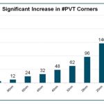
Transistor-level circuit designers have an insatiable appetite to run numerous SPICE circuit simulations in order to determine circuit speed, current and power across Process, Voltage and Temperature (PVT) conditions. Just look at the number of PVT corners increasing as the technology nodes go to 16nm:
The good news today … Read More
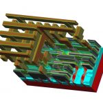
With the award of the Nobel prize for physics to Higgs (who used to work in the same building at Edinburgh as I did, reflected glory) and Englert yesterday, CERN has been in the news. ClioSoft has an interesting presentation given at CERN about designing a detector chips. The work was done two or three years ago, managed from Lawrence… Read More
There is an interesting discussion on SemiWiki in regards to the age old question aboutbenchmarking EDA tools. I remember benchmark discussions at my first DAC in 1984. It was deemed impossible to do a “fair” public benchmark then and it’s not possible now, just my opinion of course but let me tell you why. Simply stated it is a legal,… Read More
As they have done for the last few years, Atrenta held its fifth annual user group meeting at the Shin Yokohama Kokusai Hotel on September 13. The attendees are a mixture of customers and other interested members of the semiconductor supply chain. There were nearly 90 people there representing 48 different companies in Japan.
The… Read More
At this year’s DAC, I spoke with several friends at Cadence. I got the distinct impression that something at Cadence had changed. There was a sense of pride and accomplishment that it seems to me had drifted away over the years. Now employees were speaking with true conviction about the accomplishments of the product development… Read More
Electronic Design Automation Software and Semiconductor Intellectual Property are not so much the tail that wags the dog, rather they are like the heart of an elephant, tiny in comparison but without which there is no elephant. There is no doubt that EDA and IP have been key enablers of the semiconductor industry for the past 50 years… Read More
From chip IP vendor ARM Holdings to semiconductor foundry Taiwan Semiconductor, there have been many winners from the mobile device revolution that was sparked by Apple’s introduction of the iPhone. However, while these big-ticket names get all the fame and glory, the electronic design automation space (“EDA” for short) is … Read More
VIPs (Verification IPs) are really important in this complex world of SoCs which involve various IPs, interfaces and continuously evolving protocols and standards, thus making the task of verifying an overall system extremely challenging. And the verification must be done in minimum possible run-time and memory consumption.… Read More
Analog and mixed-signal ICs are tougher to design and verify compared to digital, so if you want to learn more about best practices from actual AMS engineers then consider attending a summitthat is sponsored by Cadence Design Systems next Thursday, October 10th in San Jose from 8:00AM until 6:30PM.
They’ve lined up an interesting… Read More