You are currently viewing SemiWiki as a guest which gives you limited access to the site. To view blog comments and experience other SemiWiki features you must be a registered member. Registration is fast, simple, and absolutely free so please,
join our community today!
The prevailing industry trends are clear: (1) PCB and die package designs are becoming more complex, across both mobile and high-performance applications; (2) communication interface performance between chips (and their related protocols) is increasingly demanding to verify; (3) signal integrity and power integrity issues… Read More
With the coming onslaught of IoT designs from big companies and small, the opportunity for IoT FPGA prototyping deserves a closer look. This session will start off with a keynote “The Internet of Trust and a New Frontier For Exploration” and will be followed by a discussion with industry experts Don Dingee, Frank Schirrmeister,… Read More
If you’re in the chip biz in Silicon Valley, check out the SOI Consortium FD-SOI Symposium on April 13th in San Jose. They’ve been running these things since 2009, and I have to say that this one is the most comprehensive to date. Headliners include Cisco, Sony, NXP, SigmaDesigns, ARM, Ciena plus the big FD-SOI foundries,… Read More
In many ways, static timing analysis (STA) is more of an art than a science. Methodologists are faced with addressing complex phenomena that impact circuit delay — e.g., signal crosstalk, dynamic I*R supply voltage drop, temperature inversion, device aging effects, and especially (correlated and uncorrelated) process… Read More
Whether or not in the past you believed all the of rhetoric about exploding design complexity in SOC’s, today there can be no debate that SOC size and complexity is well beyond something that can be managed without some kind of design management system. As would be expected, development of most larger designs relies on a data management… Read More
We wrote about the history of Cadence in preparation for our book “Fabless: The Transformation of the Semiconductor Industry” in 2012. EDA played a key role in enabling the fabless semiconductor revolution and Cadence was right there at the beginning. Famed EETimes editor Richard Goering helped us with the book and the Cadence… Read More
Next week I will be at DVCON which is not to be confused with DEFCON the community of black and white hat hackers that challenge our online privacy on a daily basis. DVCON is the premier conference for the functional design and verification of our beloved electronic devices. The big draw next week of course is the keynote by Dr. Walden… Read More
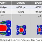
The design of parallel interfaces is supposed to be (comparatively) easy — e.g., follow a few printed circuit board routing guidelines; pay attention to data/clock/strobe signal lengths and shielding; ensure good current return paths (avoid discontinuities); match the terminating resistances to the PCB trace impedance;… Read More
2015 will be remembered as the year when chip-package-system (CPS) physical co-design and electrical/thermal analysis methodologies took center stage.… Read More
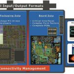
A new term has entered the vernacular of electronic design engineering — pathfinding. The complexity of the functionality to be integrated and the myriad of chip, package, and board technologies available make the implementation decision a daunting task. Pathfinding refers to the method by which the design space of technology… Read More