You are currently viewing SemiWiki as a guest which gives you limited access to the site. To view blog comments and experience other SemiWiki features you must be a registered member. Registration is fast, simple, and absolutely free so please,
join our community today!
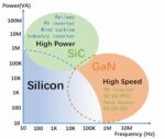
I’ve read articles about power electronics, RF systems and high-frequency applications using SiC and GaN transistors, especially in EVs and chargers, but hadn’t looked into the details of GaN devices. A recent Silvaco webinar proved to be just the format that I needed to learn more about GaN design and optimization. Udita Mittal,… Read More
In the rapidly evolving semiconductor landscape, imec’s recent breakthroughs in wafer-to-wafer hybrid bonding and backside technologies are reshaping the future of compute systems. As detailed in their article, these innovations transition CMOS 2.0 from a conceptual framework to practical reality, enabling denser,… Read More
Semiconductor fabs aim to have high yields and provide processes that attract design firms and win new design starts, but how does a fab deliver their process nodes in a timely manner without having to run lots of expensive silicon through the line? This is where simulation and TCAD tools come into play, and to learn more about this… Read More
Design-Technology Co-Optimization (DTCO) has been a foundational concept in semiconductor engineering for years. So, when Synopsys referenced DTCO in their April 2025 press release about enabling Angstrom-scale chip designs on Intel’s 18A and 18A-P process technologies, it may have sounded familiar—almost expected. … Read More
Now that the dust has settled, I will give you my take on the Intel Foundry event. Some might call me a semiconductor event critic as I have attended hundreds of them over the last 40 years starting with the Design Automation Conference in 1984. Foundry events are my favorite because they really are the pulse of the semiconductor industry,… Read More
Preventing the propagation of systematic defects in today’s semiconductor design-to-fabrication process requires many validation, analysis and optimization steps. Tools involved in this process can include design rule checking (DRC), optical proximity correction (OPC) verification, mask writing and wafer printing… Read More
The semiconductor industry’s incredible juggernaut has been powered by device innovations at its very core. Moreover, present-day enterprises encounter immense competitive pressures and innovations are a key differentiator to maintain their competitive edge1.
“It wasn’t that Microsoft was so brilliant or clever… Read More
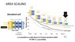
At the IEDM conference in December 2022, Imec presented “Semi-damascene Integration of a 2-layer MOL VHV Scaling Booster to Enable 4-track Standard Cells,” I had a chance to not only read the paper and see it presented, but also to interview one of the authors Zsolt Tokie.
Logic designs are built up by standard cells such as inverters,… Read More
TSMC recently held their 10th annual Open Innovation Platform (OIP) Ecosystem Forum. An earlier article summarized the highlights of the keynote presentation from L.C. Lu, TSMC Fellow and Vice-President, Design and Technology Platform, entitled “TSMC and Its Ecosystem for Innovation” (link).
One of the topics that L.C. … Read More
Spin-transfer torque magnetoresistive RAM (STT-MRAM) has emerged from several foundries as a very attractive IP option. An introduction to MRAM technology from GLOBALFOUNDRIES was provided in this earlier SemiWiki article. [1]
Briefly, STT-MRAM is a non-volatile storage option with the following attractive characteristics… Read More