You are currently viewing SemiWiki as a guest which gives you limited access to the site. To view blog comments and experience other SemiWiki features you must be a registered member. Registration is fast, simple, and absolutely free so please,
join our community today!
Alchip Technologies Ltd., a global leader in high-performance computing (HPC) and artificial intelligence (AI) ASIC design and production services, continues its trajectory of rapid growth and technical leadership by pushing the boundaries of advanced-node silicon, expanding its global design capabilities, and building… Read More
Dave Hwang joined Alchip in 2021 as General Manager of Alchip’s North America Business Unit. He also serves as Senior Vice President, Business Development. Prior to join Alchip, Dave served as Vice President, Worldwide Sales and Marketing for Global Unichip and in a variety of management and technical roles at TSMC. He holds… Read More
Anna Fontanelli, CEO of MZ Technologies, is a silicon executive with more than 35 years of expertise in managing complex R&D organizations/programs to give birth to innovative EDA technologies. Strong communication skills and proven ability to lead distributed, cross functional teams in international environments.… Read More
The semiconductor industry is facing a paradigm shift. Traditional scaling, once driven by Moore’s Law, is slowing down. For years, moving to smaller process nodes led to lower transistor costs and better performance. However, scaling from node to node now offers fewer benefits as wafer costs rise much more than the historical… Read More
Keysight, with deep roots tracing back to Hewlett-Packard, has long been at the forefront of innovation in electronic design and testing. It manufactures electronics test and measurement equipment and software. The company also owns its own foundry and makes custom chips and packages for its instrumentation business. Many… Read More
Predictions in technology adoption often hinge on a delicate balance between technical feasibility and market dynamics. While business considerations play a pivotal role, the technical category reasons for the success or failure of a prediction are more tangible and often easier to identify—if scrutinized with care. However,… Read More
A growing trend in system design is the use of multiple ICs mounted in advanced packages, especially in high-performance computing and AI. These modern packages now integrate multiple ICs, often with high-bandwidth memory (HBM), resulting in hundreds of thousands of connections that need proper verification. Traditional… Read More
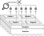
In the quest to secure the authenticity and ownership of advanced integrated circuit (IC) packages, a novel approach has been introduced in this paper that capitalizes on the inherent physical discrepancies within these components. This method, distinct from traditional strategies like physical unclonable functions (PUFs)… Read More
At the 2024 TSMC OIP Ecosystem Forum, one of the technical talks by TSMC focused on maximizing 3DIC design productivity and rightfully so. With rapid advancements in semiconductor technology, 3DICs have become the next frontier in improving chip performance, energy efficiency, and density. TSMC’s focus on streamlining the… Read More


