You are currently viewing SemiWiki as a guest which gives you limited access to the site. To view blog comments and experience other SemiWiki features you must be a registered member. Registration is fast, simple, and absolutely free so please,
join our community today!
By Hossam Sarhan
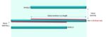
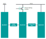
Communication has become the backbone of our modern world, driving the rapid growth of the integrated circuit (IC) industry, particularly in communication and automotive applications. These applications have increased the demand for high-performance analog and radio frequency (RF) designs.
However, designing… Read More
By Mark Tawfik
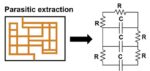
Parasitic extraction is essential in integrated circuit (IC) design, as it identifies unintended resistances, capacitances, and inductances that can impact circuit performance. These parasitic elements arise from the layout and interconnects of the circuit and can affect signal integrity, power consumption,… Read More
The week before DAC I had the privilege to take a video call with Pradeep Thiagarajan – Product Manager, Simulation, Custom IC Verification at Siemens EDA to get an update on new simulation products. I’ve been following Solido for years now and knew that they were an early adopter of ML for Monte Carlo simulations with SPICE users.… Read More
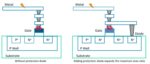
IC layouts go through extensive design rule checking to ensure correctness, before being accepted for fabrication at a foundry or IDM. There’s something called the antenna effect that happens during chip manufacturing where plasma-induced damage (PID) can lower the reliability of MOSFET devices. Layout designers run Design… Read More
Who first came up with this term shift-left ? I’d assumed Siemens EDA as they use it so widely. But their latest white paper on the productivity improvements possible with shift-left Calibre IC verification flows puts the record straight: a software engineer called Larry Smith bagged the naming rights in a 2001 paper (leapfrogging… Read More
The Siemens Calibre group was very busy last week at SPIE. Calling Calibre industry leading really is an understatement. Calibre is one of the reasons Moore’s Law has continued to this day. This tool is legendary. You can get more information on the Calibre landing page including product information, resource guide, blogs
…
Read More
IC reliability is an issue that circuit design engineers and reliability engineers are concerned about, because physical effects like high Current Density (CD) in interconnect layers, or high point-to-point (P2P) resistance on device interconnect can impact reliability, timing or Electrostatic Discharge (ESD) robustness.… Read More
My first transistor-level IC design job was with Intel, doing DRAM designs by shrinking the layout to a smaller process node, and it also required running lots of SPICE runs with manually extracted parasitics to verify that everything was operating OK, meeting the access time specifications and power requirements across PVT … Read More
Physical verification is an important and necessary step in the process to tapeout an IC design, and the foundries define sign-off qualification steps for:
- Physical validation
- Circuit validation
- Reliability verification
This sounds quite reasonable until you actually go through the steps only to discover that some of the … Read More
There are a few dozen causes of semiconductor failure. Most can be lumped into one of three categories: material defects, process or workmanship issues, or environmental or operational overstress. Even when all those causes are carefully mitigated, one factor is limiting reliability more as geometries shrink – and it… Read More