You are currently viewing SemiWiki as a guest which gives you limited access to the site. To view blog comments and experience other SemiWiki features you must be a registered member. Registration is fast, simple, and absolutely free so please,
join our community today!
What’s Testing Design Limits at ITC?by Beth Martin on 10-02-2015 at 12:00 pmCategories: EDA, Siemens EDA
The 46[SUP]th[/SUP] IEEE International Test Conference (ITC) will be held the week of October 5, 2015 at the Disneyland Hotel Conference Center in Anaheim, California. ITC is where you will discover the latest ideas and learn about practical applications of test technologies.
As you take in panels, tutorials, presentations,… Read More
In the first part of this article, I talked about some of the key business aspects along with some technical aspects like system performance, functionality, and IP integration that drive the architecture of an SoC for its best optimization and realization in an economic sense. In this part, let’s dive into some more aspects that… Read More
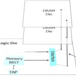
3D-IC has a stack of dies connected and packaged together, and therefore needs new testing strategies other than testing a single die. It’s given that a single defective die can render the whole of 3D-IC unusable, so each die in the stack must be completely and perfectly tested before its entry into that stack. Looking at it from a … Read More
Traditionally ATPG (Automatic Test Pattern Generation) and BIST (Built-In-Self-Test) are the two approaches for testing the whole semiconductor design squeezed on an IC; ATPG requires external test equipment and test vectors to test targeted faults, BIST circuit is implemented on chip along with the functional logic of IC.… Read More
I am talking about the health of electronic and semiconductor design, which if made sound at RTL stage, can set it right for the rest of the design cycle for faster closure and also at lesser cost. Last week was the week of ITC(International Test Conference) for the Semiconductor and EDA community. I was looking forward to what ITC… Read More
In the world of IC testability we tend to look at various approaches as independent means to an end, namely high test coverage with the minimum amount of test time, minimum area impact, minimum timing impact, and acceptable power use. Automatic Test Pattern Generation (ATPG) is a software-based approach that can be applied to any… Read More
Once upon a time, ASIC designers were integrating memories in their design (using a memory compiler being part of the design tools provided by the ASIC vendor), then they had to make the memory observable, controllable… and start developing the test program for the function, not a very enthusiastic task (“AAAA” and “5555” and other… Read More
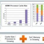
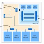
Benjamin Franklin, “I didn’t fail the test, I just found 100 ways to do it wrong.” I was reminded of this line during a joint Mentor-ARM seminar yesterday about testing ARM cores and memories. The complexity of testing modern SoC designs at advanced nodes, with multiple integrated ARM cores and other IP, opens up plenty of room for… Read More
Testing, testing… 3D ICsby Beth Martin on 10-06-2011 at 7:01 pmCategories: EDA, Siemens EDA
3D ICs complicate silicon testing, but solutions exist now to many of the key challenges. – by Stephen Pateras
The next phase of semiconductor designs will see the adoption of 3D IC packages, vertical stacks of multiple bare die connected directly though the silicon. Through-silicon vias (TSV) result in shorter and thinner… Read More
Introduction
Before DAC I met with Stephen Pateras, Ph.D. at Mentor Graphics, he is the Product Marketing Director in the Silicon Test Solutions group. Stephen has been at Mentor for two years and was part of the LogicVision acquisition. He was in early at LogicVision and went through their IPO, before that he was at IBM in the mainframe… Read More