You are currently viewing SemiWiki as a guest which gives you limited access to the site. To view blog comments and experience other SemiWiki features you must be a registered member. Registration is fast, simple, and absolutely free so please,
join our community today!
As you know, I’ve been a bit of a bear about what is happening to wafer costs at 20nm and below. At the Common Platform Technology Forum last week there were a number of people talking about this in presentations and at Harvey Jones’s “fireside chat”.
At the press lunch I asked about this. There are obviously… Read More
I was at the Common Platform Technology Forum this week. One of the most interesting sessions is IBM’s Gary Patton giving an overview of the state of semiconductor fabrication. Then, at lunchtime, he is one of the people that the press can question. In this post, I’m going to focus on Extreme Ultra-Violet (EUV) lithography.… Read More
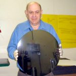
I’ve been digging around the Interwebs a bit trying to find out what the received wisdom is about how big a cost reduction can be expected if and when we transition to 450mm (18″) wafers from today’s standard of 300mm (12″). And the answers are totally all over the place. They vary from about a 30% cost reduction… Read More
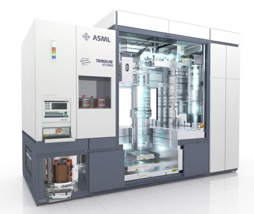
At Semicon a few weeks ago the big news was that Intel was making a big investment in ASML as a way of funding two development programs: extreme ultra-violet (EUV) and 450mm wafers. This week TSMC announced that they would join the program too, committing 275M Euros over a five year period. They are also taking a 5% stake in ASML. ASML… Read More
Behind great humor often lies irony. In the midst of a struggle by the European Union to extract $1.3B from Intel in an ages old Anti-Trust case, the latter makes a strategic move to embolden the Dutch firm ASML to accelerate the development of 450mm and EUV and thus save a continental jewel. What now say EU? When disfunction and bankruptcy… Read More
During the most recent conference call (transcript), TSMC not only beat revised estimates and announced record spending levels for 2011, Morris Chang also officially announced that a 450mm fab (Fab 12 Phase VI) is currently in the planning stages with target production @ 20nm in 2015. This is HUGE!
According to Morris Chang:
“For… Read More


