You are currently viewing SemiWiki as a guest which gives you limited access to the site. To view blog comments and experience other SemiWiki features you must be a registered member. Registration is fast, simple, and absolutely free so please,
join our community today!
The demand for high-performance computing (HPC), data centers, and AI-driven applications has fueled the rise of 2.5D and 3D multi-die designs, offering superior performance, power efficiency, and packaging density. However, these benefits come with myriads of challenges, such as multi-physics, which need to be addressed.… Read More
At the 2024 TSMC OIP Ecosystem Forum, one of the technical talks by TSMC focused on maximizing 3DIC design productivity and rightfully so. With rapid advancements in semiconductor technology, 3DICs have become the next frontier in improving chip performance, energy efficiency, and density. TSMC’s focus on streamlining the… Read More
Synopsys made significant announcements during the recent TSMC OIP Ecosystem Forum, showcasing a range of cutting-edge solutions designed to address the growing complexities in semiconductor design. With a strong emphasis on enabling next-generation chip architectures, Synopsys introduced both new technologies and … Read More
Why Glass Substrates?by Sharada Yeluri on 08-13-2024 at 6:00 amCategories: 3D IC
The demand for high-performance and sustainable computing and networking silicon for AI has undoubtedly increased R&D dollars and the pace of innovation in semiconductor technology. With Moore’s Law slowing down at the chip level, there is a desire to pack as many chiplets as possible inside ASIC packages and get … Read More
Introduction of 2.5D and 3D multi-die based products are helping extend the boundaries of Moore’s Law, overcoming limitations in speed and capacity for high-end computational tasks. In spite of its critical function within the 3DIC paradigm, the interposer die’s role and related challenges are often neither fully comprehended… Read More
At the recent User2user conference, Amit Kumar, Principal Hardware Engineer, Microsoft, shared the company’s experience from building a 3DIC SoC and highlighted Siemens EDA tools that were used. The following is a synthesis of core aspects of that talk.
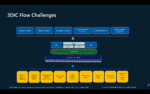
3DIC Challenges
Despite the numerous advantages of 3DIC technology, its… Read More
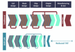
Establishing void-free fill of high aspect ratio TSVs, capped by a thin and uniform bulk layer optimized for removal by CMP, means fully optimizing each of a series of critical phases. As we will see in this 3-part series, the conditions governing outcomes for each phase vary greatly, and the complexity of interacting factors means… Read More
Establishing void-free fill of high aspect ratio TSVs, capped by a thin and uniform bulk layer optimized for removal by CMP, means fully optimizing each of a series of critical phases. As we will see in this 3-part series, the conditions governing outcomes for each phase vary greatly, and the complexity of interacting factors means… Read More
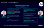
In today’s rapidly advancing technological landscape, semiconductors are at the heart of innovation across diverse industries such as automotive, healthcare, telecommunications, and consumer electronics. As a leader in technology and engineering, Siemens plays a pivotal role in empowering the next generation … Read More
In today’s rapidly evolving semiconductor industry, the design and integration of intellectual property (IP) play a pivotal role in achieving competitive advantage and market success. Whether sourced from commercial IP providers or developed in-house, ensuring that IP designs are compliant with signoff requirements… Read More