As semiconductors continue to scale, designers are turning to 3DIC architectures to meet increasing demands for performance, energy efficiency, and functional density in data centers and edge AI applications. However, stacking multiple dies introduces new multiphysics challenges including electrical, structural, and… Read More
Themed Heterogeneous Integration: Bolstering Europe’s Resilience the 3D & Systems Summit 2025 will primarily focus on exploring strategies for enhancing Europe’s semiconductor industry addressing topics as geopolitical dynamics, market trends, as well as the latest advancements in chiplet applications… Read More
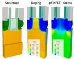
Semiconductor fabs aim to have high yields and provide processes that attract design firms and win new design starts, but how does a fab deliver their process nodes in a timely manner without having to run lots of expensive silicon through the line? This is where simulation and TCAD tools come into play, and to learn more about this… Read More
3D design with high-bandwidth memory stacks (HBM) has become essential for leading edge semiconductor systems in multiple applications. Hyperscalers depend on large AI accelerator cores supported by 100GB or more of in-package HBM to handle trillion parameter AI models. Autonomous Drive (AD) vehicles may handle smaller … Read More
Introduction of 2.5D and 3D multi-die based products are helping extend the boundaries of Moore’s Law, overcoming limitations in speed and capacity for high-end computational tasks. In spite of its critical function within the 3DIC paradigm, the interposer die’s role and related challenges are often neither fully comprehended… Read More
For a long time, package engineering was part of the cleanup crew for chip design. The glory was all around the design of advance monolithic chips on the latest technology node. Once the design was done, the package/test team would take the design over the finish line, adding the required I/O specs, lead frame, load board and test … Read More
Intel recently issued a press announcement that has significant implications for the future of semiconductors. The release announces Intel’s new glass substrate technology. The headline states: Glass substrates help overcome limitations of organic materials by enabling an order of magnitude improvement in design rules… Read More
It was refreshing to hear a talk focused on emerging stronger from the downturn when the news and media are focused on the gloom. At the recent Siemens EDA User2User conference, Joe Sawicki, executive vice president, IC, gave an uplifting keynote talk to the audience. He highlighted a secular growth trend happening in the semiconductor… Read More


