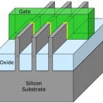
In the semiconductor industry, it feels great to hear about the process technology shrinking to lower nodes along with innovative transistor structures that offer major gains in PPA (Power, Performance and Area). However, it requires huge investment of capital, time and effort from foundries to conceptualize, prototype and… Read More
Tag: 22nm
Handel Jones Predicts Process Roadmap Slips
At the SEMI ISS conference earlier this week, the last speaker in the technology challenges section was Handel Jones of IBS. I’ve known Handel since the mid-1980s when he came to VLSI Technology and told us we were losing money on 90% of the designs we were doing but our cost model was not good enough and so we didn’t even… Read More
New Frontiers in Scan Diagnosis
As we move down into more and more advanced process nodes, the rules of how we test designs are having to change. One big challenge is the requirement to zoom in and fix problems by doing root cause analysis on test data alone, along with the rest of the design data such as detailed layout, optical proximity correction and so on. But without… Read More
The Rosetta Stone of Lithography
At major EDA events, CEDA (the IEEE council on EDA, I guess you already know what that bit stands for) hosts a lunch and presentation for attendees and others. This week was ICCAD and the speaker was Lars Liebmann of IBM on The Escalating Design Impact of Resolution-Challenged Lithography. Lars decided to give us a whirlwind tour … Read More
Are 28nm Transistors the Cheapest…Forever?
It is beginning to look as if 28nm transistors, which are the cheapest per million gates compared to any earlier process such as 45nm, may also be the cheapest per million gates compared to any later process such as 20nm.
What we know so far: FinFET seems to be difficult technology because of the 3D structure and so the novel manufacturing… Read More
Rapid Yield Optimization at 22nm Through Virtual Fab
Remember? During DAC2013 I talked about a new kind of innovation: A Virtual Fabrication Platform, SEMulator3D, developed by COVENTOR. Now, to my pleasant surprise, there is something to report on the proven results from this platform. IBM, in association with COVENTOR, has successfully implemented a 3D Virtual Fabrication… Read More
Intel Is Continuing to Scale While Others Pause
Back in May, William Holt, EVP of technology and manufacturing at Intel gave a presentation to analysts entitled Advancing Moore’s Law, Imperatives and Opportunity. A pdf of the presentation is available here. I just saw it for the first time today and I’m not sure how to get my head around it. It starts off with a lot … Read More
Intel’s New Tablet Strategy Brings Ivy Bridge to the Forefront
In an article published this week in microprocessor report and highlighted in Barron’s, Linley Gwennap makes the argument that Intel should stay the course and fix the PC instead of trying to offset its declines with sales into the Smartphone and Tablet space. He cites that lower PC sales growth was due to a dramatic slowdown in processor… Read More
How Apple Plans to Leverage Intel’s Foundry
Tim Cook’s strategy to disengage from Samsung as a supplier of LCDs, memory and processors while simultaneously creating a worldwide supply chain from the remnants of former leaders like Sharp, Elpida, Toshiba and soon Intel is remarkable in its scope and breadth. By 2014, Apple should have in place a supply chain for 500M iOS devices… Read More
Will Paul Otellini Convince Tim Cook to Fill Intel’s Fabs?
An empty Fab is a terrible thing to waste, especially when it is leading edge. By the end of the year Intel will, by my back of the envelope calculation, be sitting with the equivalent of one idle 22nm Fab (cost $5B). What would you do if you were Paul Otellini?
Across the valley, in Cupertino, you have Tim Cook, whose modus operandi is … Read More


