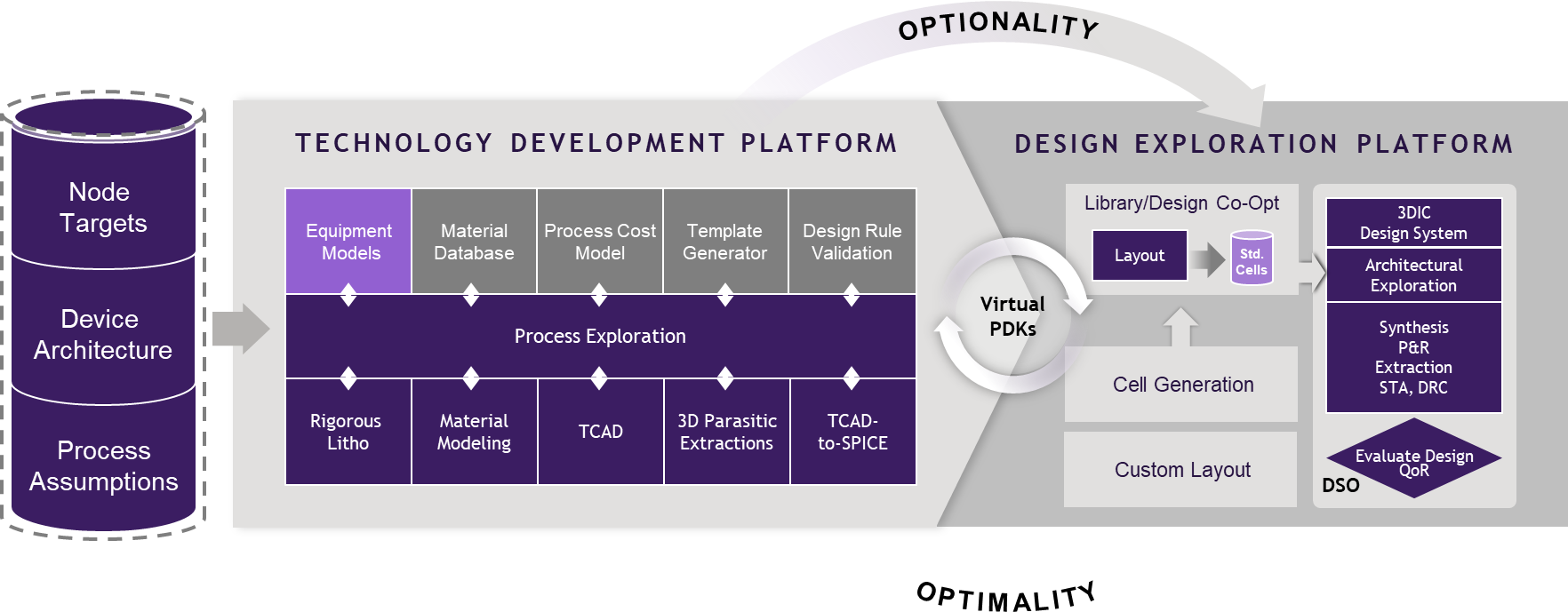
Our good friend Scotten Jones wrote a paper on a product that has been in joint development with Synopsys and is now available. Scott is currently President Semiconductor Manufacturing Economics and Senior Fellow at TechInsights. Scott and I have discussed this product many times and I feel it is ground breaking technology for semiconductor design. Scott briefed me on it at IEDM and sent me the white paper. Here is my take on it:

The semiconductor industry is shifting from traditional Power, Performance, and Area (PPA) metrics to a broader PPACtE framework, incorporating Cost (C), Cycle Time (t), and Environmental impact via Carbon Equivalents (E). Synopsys’ DTCO suite has long facilitated TCAD-based PPA optimization. TechInsights’ Cost Explorer plug-in integrates into Synopsys Sentaurus Process Explorer, enabling full PPACtE analysis. This tool has been demonstrated by Tokyo Electron to assess CFET architectures, revealing a 15.3% cost premium for sequential over monolithic designs. With node development costs exceeding billions, Cost Explorer promises substantial savings in R&D and manufacturing by simulating CtE alongside PPA before physical prototyping.
Introduction
For decades, semiconductor advancements focused on PPA improvements, as seen in TSMC’s 3nm node offering 25-30% power reduction, 10-15% performance boost, and 70% density gain over 5nm. However, escalating costs, extended cycle times, and environmental concerns—highlighted by industry leaders like TSMC and Applied Materials—demand inclusion of CtE. With 3nm/2nm R&D nearing $10 billion per node, early simulation is crucial. DTCO co-optimizes design and process, but traditional tools like Synopsys’ suite lack CtE modeling. TechInsights’ Cost Explorer addresses this, enhancing Synopsys’ ecosystem for comprehensive PPACtE optimization, as proven in CFET studies.
New Technology Development
Semiconductor node development spans two phases: initial simulation-driven optimization of devices, models, and flows to meet PPA, followed by test chip fabrication and PDK refinement. TCAD minimizes costly wafers by iterating assumptions virtually. Synopsys DTCO excels here but omits CtE, limiting holistic optimization.
Synopsys DTCO Solution
Synopsys’ DTCO flow integrates tools like Proteus for patterning, QuantumATK for materials, Sentaurus TCAD for architectures, and Fusion Technology for design evaluation. Benefits include accurate pre-wafer simulations, realistic context feedback, and variation-aware modeling for reliable PPA. Collaboration with TechInsights adds CtE metrics, expanding design evaluation.
Synopsys Sentaurus Process Explorer
This tool enables interactive 3D visualization, process debugging, and metrology for advanced nodes like FinFETs and GAA. Features support yield analysis, anomaly detection, and TCAD integration, reducing cycle time and enhancing collaboration. It accelerates DTCO by identifying issues early, maximizing simulation ROI.
CtE Modeling Requirements
CtE estimation demands detailed fab and process modeling. Cost varies by fab capacity, location, and steps, calculated via equipment, labor, materials, and facilities. Cycle time uses ideal estimates (step-by-step processing) multiplied by an Xideal factor for realism. Carbon footprint tracks material usage, emissions, and abatement. Cost Explorer computes these from process flows.
How Cost Explorer Works
Users define fab parameters (country, capacity, node) and build flows by selecting from 93 equipment types, parameterizing steps (e.g., film thickness). Pre-populated tables handle configurations, throughputs, costs, and materials. Algorithms compute equipment needs, costs (wafers, labor, depreciation), ideal cycle time, and carbon via GWP factors. Outputs include per-step breakdowns, as in Samsung 3nm GAA analysis.
Integration with Sentaurus Process Explorer
In Process Explorer, users assign equipment to steps, triggering Cost Explorer to auto-populate and calculate CtE. Results display per step and total, enabling iterative PPACtE refinement within the DTCO flow.
Use Cases
Tokyo Electron’s 2023 VLSI study used an early Cost Explorer to compare CFETs: monolithic (better performance, area) vs. sequential (3% lower performance, 6% higher power, 15.3% higher cost). Future work includes 2nm nanosheet evaluations with/without backside power, incorporating tE.
Bottom line: Cost Explorer’s integration into Synopsys DTCO empowers pre-wafer PPACtE optimization, slashing development costs and yielding efficient, sustainable processes. In a billion-dollar R&D landscape, this yields significant long-term savings in manufacturing, time, and emissions.
Also Read:
How PCIe Multistream Architecture Enables AI Connectivity at 64 GT/s and 128 GT/s
WEBINAR: How PCIe Multistream Architecture is Enabling AI Connectivity
Lessons from the DeepChip Wars: What a Decade-old Debate Teaches Us About Tech Evolution
Share this post via:


Comments
There are no comments yet.
You must register or log in to view/post comments.