By Nikhil Sharma, Sunghwan Son, Paul Mantey
The semiconductor industry faces an unprecedented crisis that threatens the very foundation of technological innovation. According to the latest Siemens EDA / Wilson Research Study, first-silicon success rates have plummeted to just 14%[1]—the lowest figure in more than twenty years of tracking this data. This isn’t merely a statistical anomaly; it represents a fundamental breakdown in our ability to deliver working silicon on schedule. Re-spins can range in costs depending on node-size and type of fix can range from $15M+ at 7nm to >$100M at 3nm for a full re-spin.[2]
The crisis deepens as the industry pushes toward 2nm process nodes, where the complexity of testing and ensuring manufacturability increases exponentially. Advanced node designs demand unprecedented compute and memory resources for verification workflows, making traditional on-premises infrastructure increasingly inadequate.
As recent industry analysis has highlighted, addressing this crisis requires robust data infrastructure that enables mobility, security, and availability—the foundational pillars for next-generation verification approaches. The question isn’t whether to move to the cloud—it’s how to architect the complete ecosystem that makes AI-enhanced, 2nm-capable verification possible.
Beyond Data Infrastructure – The Complete Cloud Ecosystem
AWS and NetApp together deliver the complete ecosystem demanded by 2nm-era semiconductor development. While NetApp’s FSx for NetApp ONTAP provides the high-performance, globally accessible storage foundation with FlexCache technology for seamless data mobility and FlexClone capabilities for instant environment provisioning, AWS contributes the elastic compute, advanced networking, and AI/ML services that transform how verification workflows operate at scale.
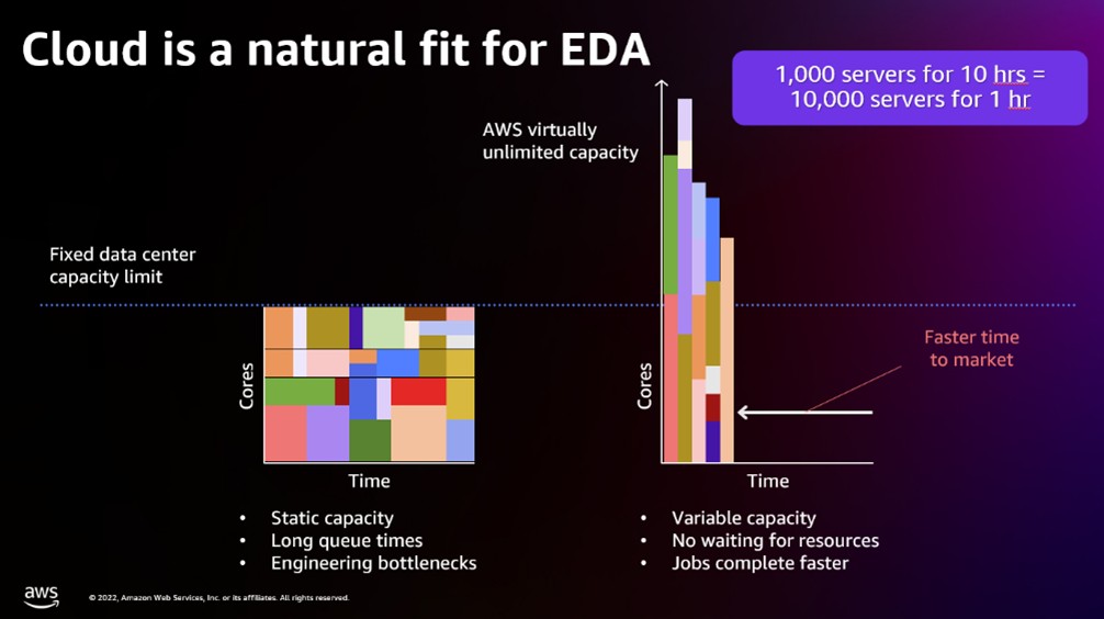
This partnership addresses the memory-intensive reality of advanced node verification. As semiconductor devices increase in density and complexity, physical verification requires compute nodes with increasingly high memory-to-core ratios and larger numbers of high-performance cores. Traditional on-premises infrastructure cannot economically provide the burst capacity that advanced verification workflows demand.
The complete transformation extends far beyond “bigger HPC jobs” to encompass four integrated capabilities:
- Elastic Resource Scaling that eliminates capital expenditure constraints,
- Accelerated Modernization with access to the latest AMD and Intel-based instances optimized for EDA workloads,
- Global Collaboration through secure chambers built on AWS infrastructure with NetApp’s global data fabric, and
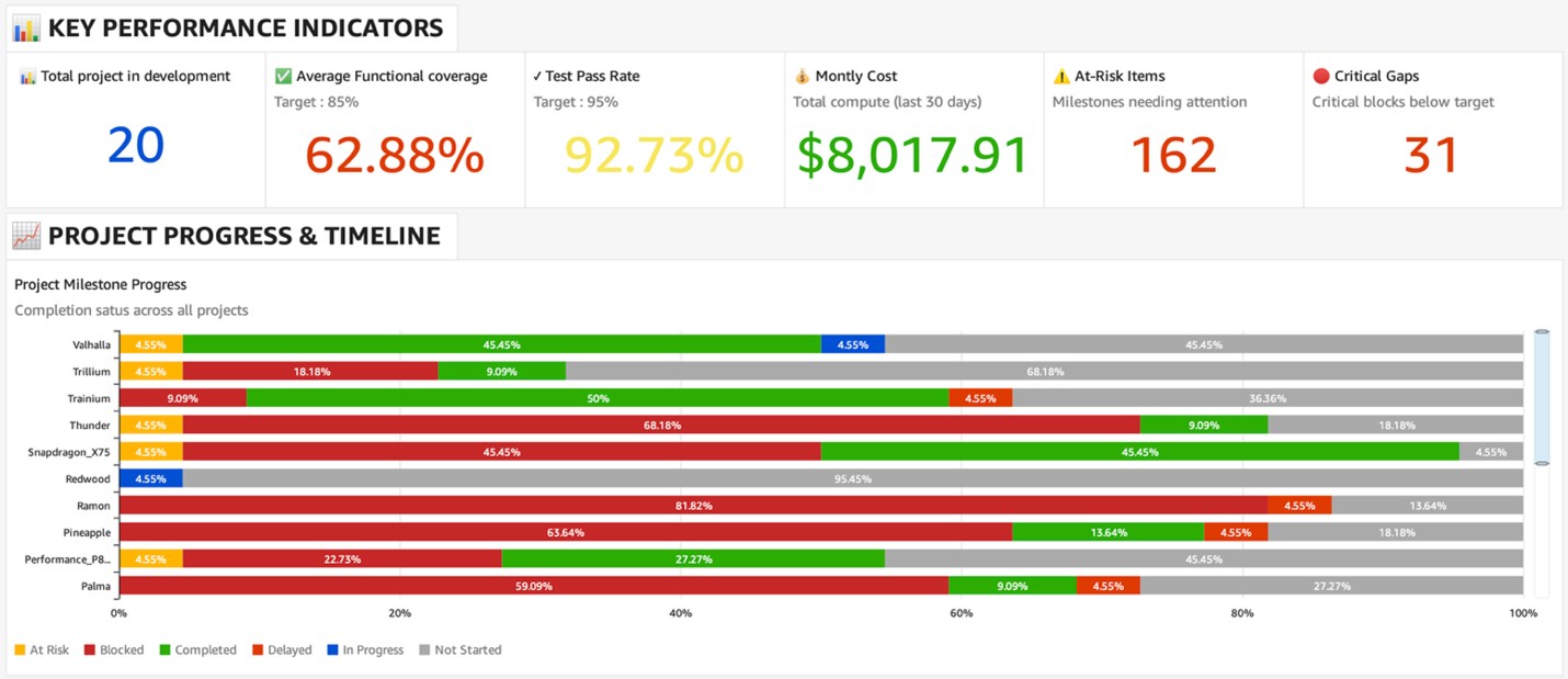
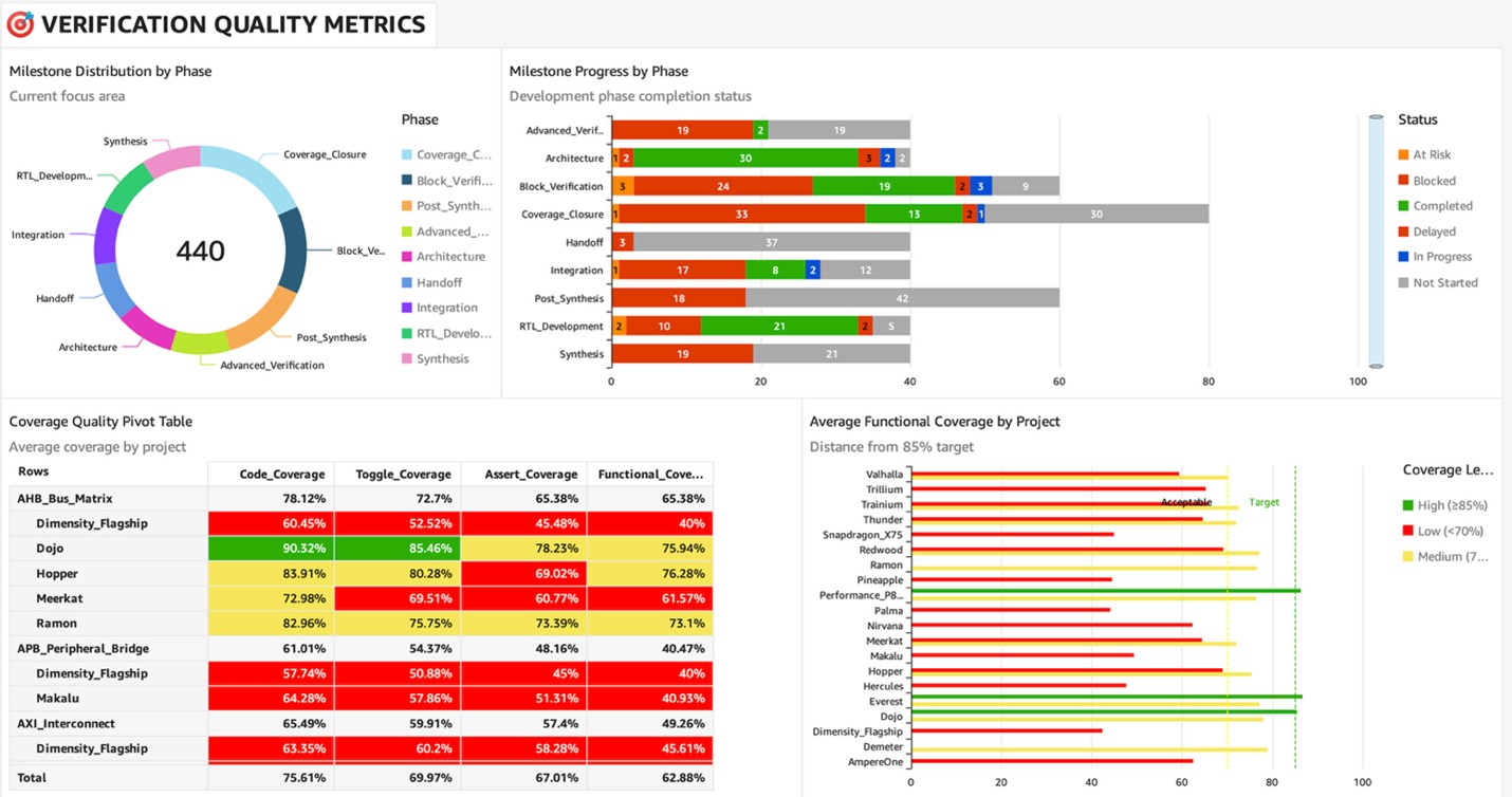
- Compressed Feedback Cycles via real-time analytics dashboards.
Modern EDA workflows require seamless integration across multiple tools, massive parallel-processing capabilities and the ability to handle the petabyte-scale datasets. Cloud environments provide the infrastructure elasticity to scale from hundreds to thousands of cores within minutes, enabling verification teams to meet aggressive project timelines without the months-long hardware procurement cycles that plague on-premises deployments.
The Analytics Foundation for AI Optimization
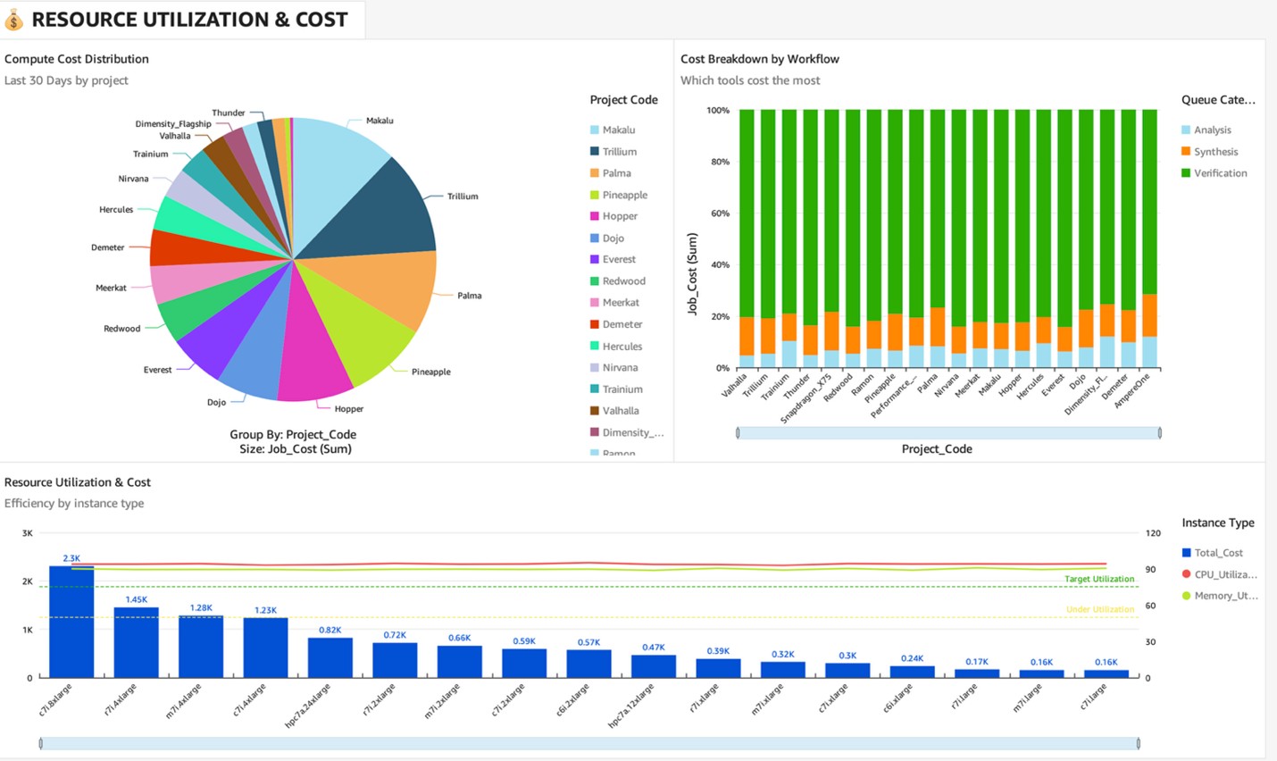
Cloud environments enable comprehensive data collection from verification runs, resource utilization patterns, coverage metrics, and performance benchmarks—creating rich datasets for analytics and optimization. This data foundation becomes the cornerstone for implementing AI-driven optimization that can fundamentally transform verification efficiency.
Real-Time Analytics Layer: Interactive dashboards provide immediate visibility into verification progress, bottleneck identification, and resource efficiency metrics. Teams can track coverage analysis, debug cycle times, and project completion status in real-time, enabling rapid course corrections with near immediate feedback loops.

AI-Driven Optimization Potential: With robust analytics foundations in place, AI systems can analyze verification patterns to optimize resource allocation, predict potential bottlenecks, and suggest configuration improvements. This creates opportunities for continuous improvement loops that learn from each verification cycle, identifying optimal tool configurations, predicting resource needs based on design complexity, and automatically adjusting compute allocation to minimize both time and cost.
Data-Driven Decision Making: The comprehensive analytics enable engineering teams to make informed decisions about resource allocation, tool selection, and verification strategies based on actual performance data rather than estimates. For instance, determining the value of specific regression tests requires the ability to measure not only improvement in coverage or bugs identified, but also the cost of running that test.


Advanced analytics can correlate design characteristics with verification resource requirements, enabling predictive capacity planning and automated scaling decisions. This intelligence layer transforms reactive verification management into proactive optimization, directly addressing the root causes behind the industry’s 14% first-silicon success challenge.
Security and IP Protection – Enterprise-Grade Implementation
The semiconductor industry’s IP protection concerns are addressed through enterprise-grade security implementations that often exceed on-premises capabilities. AWS provides hardware root-of-trust, comprehensive compliance certifications, and secure collaboration chambers enabling distributed teams, IP partners, and foundries to work together while maintaining strict access controls. AWS is compliant with ISO/IEC 270001, ITAR, AICPA SOC 2. Please refer to AWS documentation for a full list compliance programs.
NetApp’s FSx for ONTAP enhances security through FlexCache technology that enables global data access without compromising IP boundaries, and FlexClones that provide instant, isolated environment provisioning for different verification runs. These capabilities ensure that sensitive design data remains protected while enabling the collaboration essential for complex SoC development.
The security architecture implements zero-trust principles with granular access controls, encrypted data transmission, and comprehensive audit trails. Multi-tenant isolation ensures that even within shared cloud infrastructure, each project maintains complete data separation and access control.
Advanced threat detection and automated response capabilities provide continuous monitoring for potential security incidents. This comprehensive security framework often provides superior protection compared to traditional on-premises environments, where security updates and monitoring may lag behind current threat landscapes.
The Path Forward – Measurable Transformation
The semiconductor industry stands at an inflection point. The 14% first-silicon success rate represents a fundamental challenge that demands transformation. Companies that embrace the complete AWS and NetApp ecosystem gain access to elastic scaling that handles advanced verification complexity, analytics foundations that enable data-driven optimization, and security implementations that protect valuable IP.
Implementation Roadmap: Organizations can begin their transformation with pilot projects that demonstrate immediate value while building confidence in cloud-native approaches. The migration typically follows a phased approach: assessment and planning, pilot implementation, gradual workload migration, and full ecosystem optimization.

ROI Considerations: Early adopters report significant improvements in verification cycle times, resource utilization efficiency, and team collaboration effectiveness. The transformation addresses core industry challenges: verification complexity at advanced nodes, resource allocation inefficiencies, collaboration barriers across global teams, and the need for faster feedback cycles. By accelerating innovation rates and improving on-schedule metrics with AWS, these early adopters are earning more design wins and seeing significant growth in both revenue and profits.
Future Outlook: As verification requirements continue to grow with advanced process nodes, cloud-native EDA workflows provide the foundation for addressing the industry’s silicon success challenges. The integration of AI-driven optimization with comprehensive analytics creates a continuous improvement cycle that becomes more effective over time.
The future belongs to companies that recognize cloud transformation as the foundation for next-generation semiconductor development that can address the industry’s fundamental verification challenges. Success in the 2nm era and beyond requires not just better tools, but completely reimagined workflows leveraging the full potential of cloud-native architectures.
Disclaimer:
The views and opinions expressed on this blog are solely those of the author(s) and do not represent the views or positions of any employer, organization, or entity with which the author is or has been affiliated. This blog is a personal platform, and all content is shared in the author’s individual capacity.
Authors:
Nikhil Sharma is a Solutions Architecture Leader at Amazon Web Services (AWS), where he and his team of Solutions Architects help customers solve critical business challenges using AWS cloud technologies and services. With 25+ years of industry experience, Nikhil specializes in enterprise architecture and innovation. He is passionate about helping organizations leverage cloud technology to drive business outcomes.
Sunghwan Son is a Senior Solutions Architect at Amazon Web Services (AWS) who brings 17 years of distinguished experience in semiconductor design and cloud computing technologies. He specializes in optimizing Electronic Design Automation (EDA) infrastructure and developing innovative cloud solutions for enterprise customers.
Paul Mantey, FSxN Sales Specialist – High Tech, EDA & Semiconductors, NetApp, Inc. Leads a team focused on enabling builders and developers across the High-Tech, EDA and Semiconductor Development segments. Prior to joining NetApp, Paul worked 13 years at Hewlett-Packard holding various roles in Design Engineering, Enterprise Architecture, Virtualization Program Management, and Product Development. His thirteen patents represent extensive contributions to systems architecture, integration testing, and management hardware design.
References:
[1] https://resources.sw.siemens.com/en-US/white-paper-2024-wilson-research-group-ic-asic-functional-verification-trend-report/
[2] https://www.allpcb.com/allelectrohub/chip-design-and-tapeout-key-processes-explained#:~:text=Tapeout%20costs%20and%20wafer%20pricing,-Mask%20costs%20and&text=Typical%20tapeout%20cost%20estimates%20by,nm%20may%20exceed%20$100%20million.
Also Read:
Semiconductors Up Over 20% in 2025
WEBINAR: Is Agentic AI the Future of EDA?
Live Webinar: Considerations When Architecting Your Next SoC: NoC with Arteris and Aion Silicon
Share this post via:


Musk’s Orbital Compute Vision: TERAFAB and the End of the Terrestrial Data Center