You are currently viewing SemiWiki as a guest which gives you limited access to the site. To view blog comments and experience other SemiWiki features you must be a registered member. Registration is fast, simple, and absolutely free so please,
join our community today!
In this webinar, Google Cloud and NetApp explore how semiconductor companies can address the growing infrastructure demands of modern Electronic Design Automation (EDA) workflows. As process technologies continue to advance and chip designs become increasingly complex, engineering teams require scalable, high-performance… Read More
This is a live panel with industry experts who are on the leading edge of AI in semiconductor manufacturing. This is a must attend event for all levels of semiconductor professionals. I hope to see you there.
The semiconductor industry faces unprecedented challenges as it pushes toward advanced nodes below 3nm, managing exponential… Read More
By Nikhil Sharma, Sunghwan Son, Paul Mantey
The semiconductor industry faces an unprecedented crisis that threatens the very foundation of technological innovation. According to the latest Siemens EDA / Wilson Research Study, first-silicon success rates have plummeted to just 14%[1]—the lowest figure in more than twenty… Read More
The EDA (Electronic Design Automation) and semiconductor industries are experiencing a transformative shift—one that’s being powered by the rise of Agentic AI. If you attended this year’s SNUG, CDNLive, and/or DAC 2025, you couldn’t miss it: agentic AI was the hot topic, dominating keynotes, demos, and booth conversations… Read More
On July 9, 2025, Derren Dunn from IBM Research’s TJ Watson Research Center delivered a DACtv presentation, as seen in the YouTube video detailing IBM’s EDA-as-a-Solution platform. This innovative offering leverages IBM’s high-performance computing (HPC) cloud to deliver hybrid and cloud-only infrastructure for electronic… Read More
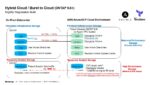
After many years of hesitancy to jump with both feet in, semiconductor companies are seriously considering implementing cloud strategies and making required investments. Their concern though is, how much investment is it going to take? Some of the block-and-tackle challenges they face in implementing a cloud strategy are … Read More
This blog is a follow-on piece to an earlier one titled NetApp’s ONTAP Enables Engineering Productivity Boost. If you have not had an opportunity to read that blog, please do so for context. Using real life examples, it showcases how customers could improve real-world design engineering productivity as much as 10%.
For the … Read More
Dan and Mike are joined by Michael Johnson (MJ), CTO at NetApp. MJ provides “behind the scene” insights into NetApp technology and how it has quietly revolutionized information storage and management for chip design. The key enabling technologies along with specific use cases are discussed. MJ also discusses moving… Read More
One of the few things that remain constant in the engineering world is the desire for higher productivity. Innovation happens when engineers are designing something and creative ideas crop up when they are reviewing and analyzing the results. In between these fun steps, engineers have to deal with the necessary evil of creating… Read More
Why burst EDA workloads to the cloud
Time to market challenges are nothing new to those of us who have worked in the semiconductor industry. Each process node brings new opportunities s along with increasingly complex design challenges. 7nm, 5nm and 3nm process nodes have introduced scale, growth, and data challenges at a level… Read More