





How VSORA rebalances memory and compute for AI inference in the data center and at the edge
For more than a decade, the AI hardware industry focused mainly on model training, while inference represented a smaller share of overall demand. That balance is changing as trained models are deployed widely in recommendation engines, content-generation systems, transcription and translation services, and autonomous devices. Industry estimates now place inference at most data-center AI workloads.
The growth of inference is changing how processor performance should be measured. Peak FLOPS alone no longer provide an adequate measure. What matters is the useful throughput a system can deliver within limits on latency, power, memory, and cost. These factors determine system capacity, operating economics, and the user’s experience.
This change exposes a mismatch between established AI processors and the requirements of inference. Most existing platforms were developed to accelerate the dense, highly parallel floating-point operations used in model training. Inference places greater demands on data movement, must handle workloads that change quickly, and often operates under strict latency limits. It must also run efficiently in both data centers and edge devices. Hardware designed mainly for training may therefore be poorly suited to delivering answers.
The Changing Computation Profile of AI Inference
Training and inference place different demands on a processor. Both involve substantial computation and data movement, but they are measured differently. Training emphasizes aggregate throughput and the time required to complete a large job, usually with large, regular batches. Inference places more emphasis on useful throughput, predictable latency, efficient use of memory, and operating cost under workloads that can vary from one request to the next.
The main differences concern latency, timing predictability, numerical precision, power and cost, and memory access.
Latency Sensitivity
Training can generally tolerate high latency for an individual operation because the objective is to process as much data as possible over the full training run. Inference, especially in interactive applications, must respond within a predictable time. Conversational systems need a short time to first token and a low delay between successive tokens. Perception and control systems may have firm deadlines. Average latency is therefore not enough; consistency and tail latency also matter.
Timing Predictability
Timing predictability is related to latency, but it is not the same measure. Two systems may have the same average latency while differing greatly in the range of response times. That range determines whether a service meets its latency target or a control loop meets its deadline. Predictable timing is therefore an architectural goal. It depends on how consistently the processor moves data and schedules work.
Numerical Precision
Precision requirements also differ. Training commonly uses mixed-precision arithmetic—for example, FP32 for selected operations and BF16, FP16, or TF32 for much of the remaining computation—to maintain numerical stability while the model learns. Inference does not update the model parameters and can often use lower precision. INT8, FP8, INT4, or FP4 can reduce model size, memory traffic, and energy use, provided that model accuracy remains acceptable.
Power and Cost
Power and cost become especially important in inference. Training concentrates a large amount of computation into a finite run, even if that run takes weeks or months. Inference operates continuously and may serve millions of requests over a model’s deployed life. Small inefficiencies are repeated on every request. Hardware utilization, energy efficiency, and cost per useful output therefore have a direct effect on operating expense.
Memory-access Behavior
Memory behavior is often the most important difference. During transformer inference, the processor must repeatedly access the model weights and key-value cache. Autoregressive decode may perform relatively little computation for each byte moved, particularly at low batch sizes. Under these conditions, performance depends more on memory bandwidth, capacity, and efficient data movement than on peak arithmetic throughput.
Most current models are too large to fit entirely in on-chip SRAM or cache, so their parameters must be fetched from high-bandwidth memory and sometimes moved across several devices. Every step through the memory hierarchy consumes time and energy. When data cannot reach the arithmetic units quickly enough, those units sit idle and delivered throughput falls.
Not all inference is memory-bound. Prompt processing, or prefill, can be compute-intensive, especially with long inputs and large batches. Token-by-token decode, however, is often limited by memory bandwidth. The balance depends on batch size, sequence length, model architecture, quantization, caching strategy, and serving software.
Peak throughput therefore tells only part of the inference-performance story. The more useful measure is the work completed within stated limits on latency, power, memory, and cost. Processor design must focus on keeping the arithmetic units supplied with data, not simply on increasing their theoretical capacity.
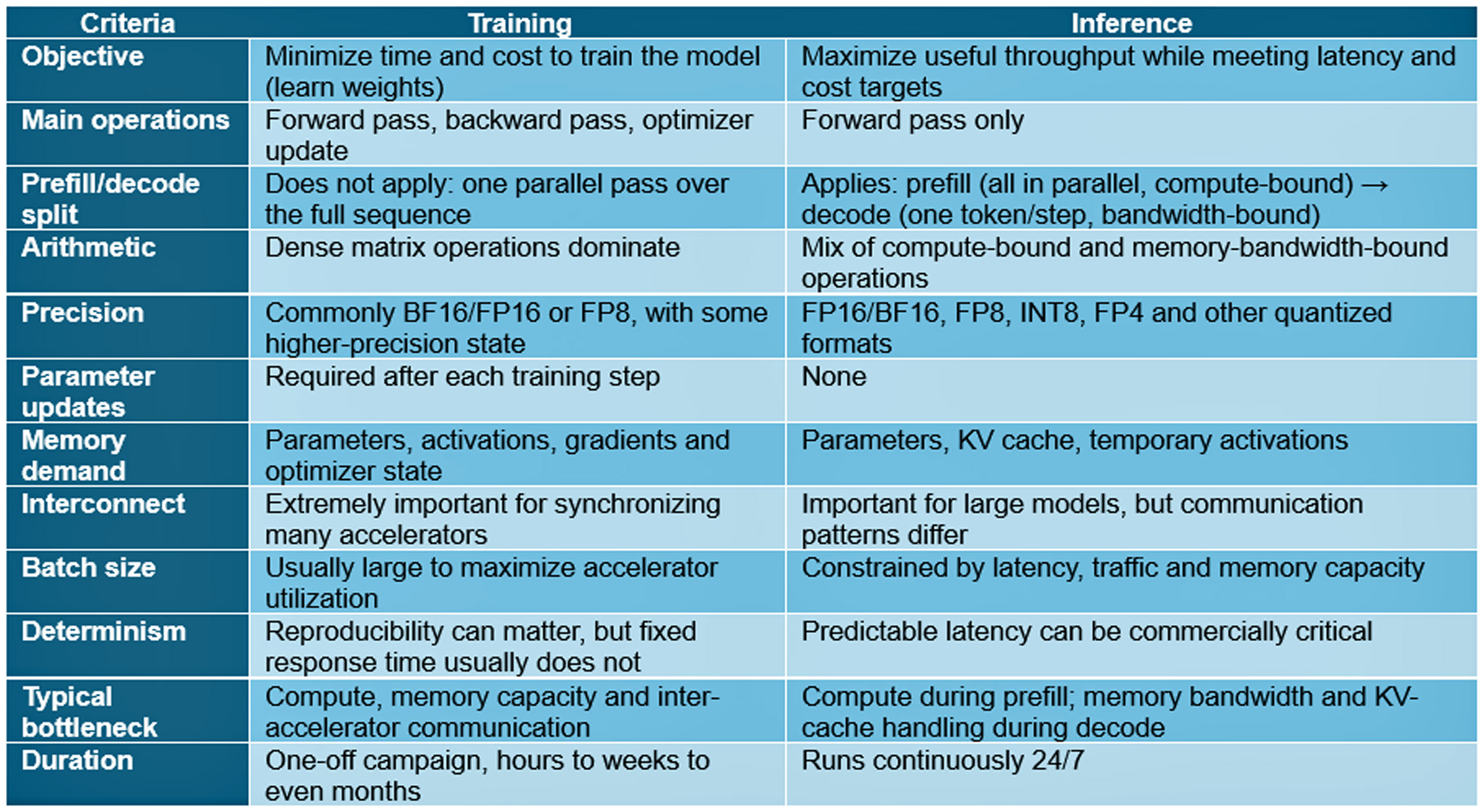
Table I captures the main differences between training and inference.
| Criteria | Training | Inference |
| Objective | Minimize time and cost to train the model (learn weights) | Maximize useful throughput while meeting latency and cost targets |
| Main operations | Forward pass, backward pass, optimizer update | Forward pass only |
| Prefill/decode split | Does not apply: one parallel pass over the full sequence | Applies: prefill (all in parallel, compute-bound) → decode (one token/step, bandwidth-bound) |
| Arithmetic | Dense matrix operations dominate | Mix of compute-bound and memory-bandwidth-bound operations |
| Precision | Commonly BF16/FP16 or FP8, with some higher-precision state | FP16/BF16, FP8, INT8, FP4 and other quantized formats |
| Parameter updates | Required after each training step | None |
| Memory demand | Parameters, activations, gradients and optimizer state | Parameters, KV cache, temporary activations |
| Interconnect | Extremely important for synchronizing many accelerators | Important for large models, but communication patterns differ |
| Batch size | Usually large to maximize accelerator utilization | Constrained by latency, traffic and memory capacity |
| Determinism | Reproducibility can matter, but fixed response time usually does not | Predictable latency can be commercially critical |
| Typical bottleneck | Compute, memory capacity and inter-accelerator communication | Compute during prefill; memory bandwidth and KV-cache handling during decode |
| Duration | One-off campaign, hours to weeks to even months | Runs continuously 24/7 |
Table I: Main differences between training and Inference based on a set of criteria
VSORA’s Architectural Innovations
VSORA starts from a different architectural background. Drawing on digital signal-processing techniques, the company designed its architecture for inference rather than adapting a platform originally built for general-purpose parallel computing. Its main target is the memory wall: the widening gap between the rate at which arithmetic units can perform calculations and the rate at which memory can supply data. VSORA coordinates computation, memory access, and data movement in an effort to keep its arithmetic resources working for more of each execution cycle.
The following sections describe its on-chip memory, support for work beyond neural-network operations, software stack, and chiplet-based scaling.
VSORA’s Architecture Targets the Memory Wall
One of VSORA’s main departures from conventional designs is its treatment of on-chip memory. GPUs distribute data among registers, shared memory, caches, and external high-bandwidth memory, each with different capacity, bandwidth, and latency. VSORA instead exposes its on-chip working memory through what the company calls a single, large register file.
This is not a conventional register file made entirely from flip-flops. It is a programming abstraction implemented with a large on-chip SRAM structure. VSORA says that the compute resources can directly address every location with single-cycle throughput. Data already in the on-chip working set can therefore be retrieved without passing through a conventional cache hierarchy.
The design has features of both scratchpad memory and compute-near-memory systems. A GPU relies on hardware-managed caches to retain and replace data in response to observed access patterns. VSORA instead uses the compiler to schedule data placement, movement, and computation explicitly. This reduces the timing variation caused by cache hits, misses, and replacement decisions. Once the compiler sets the movement and placement of data, execution time becomes more predictable. That predictability helps an inference system control tail latency rather than merely improve its average response time.
The expected benefit is a more reliable supply of operands to the arithmetic units. By coordinating data movement with execution, the architecture aims to reduce pipeline stalls and increase sustained compute utilization. This is especially relevant during autoregressive decode, when low arithmetic intensity often leaves GPU resources waiting for model weights and other data. VSORA reports sustained utilization above 50% for large-language-model inference.
That figure depends on the model, precision, batch size, sequence length, inference phase, software stack, and the way utilization is defined. Independent tests using matched workloads would be needed to verify the comparison with conventional GPUs.
Extending the Architecture Beyond AI
VSORA’s compute engine is its Matrix Processing Unit, or MPU. Its 16,384-bit-wide output datapath lets an instruction operate on a large amount of data in parallel pipelines. Programmable tensor operations are built into the MPU’s processing pipelines, and execute AI, digital signal processing (DSP), and general-purpose code. An instruction can use those pipelines in vector mode, where individual lanes work on separate data elements, or in matrix/tensor mode, where they perform operations on multidimensional data. The two modes can be interleaved in the instruction stream. That matters for workloads that mix steps such as neural-network inference and signal processing: the work can move between vector and tensor operations within the same engine, rather than being divided between a general-purpose core and a separate matrix accelerator.
This design delivers two main advantages.
The first is its suitability for edge systems, where a complete application rarely consists of AI inference alone. An autonomous-driving platform, for example, may run neural networks together with radar and lidar processing, sensor fusion, filtering, localization, image transformation, and vehicle-control algorithms. Handling these functions on one device can reduce the need for separate processors, limit chip-to-chip data transfers, and simplify the system.
The second advantage applies to neural-network inference itself. Operations used for next-token selection, such as randomized top-k sampling, can run inside the MPU. This avoids the transfers to a host processor that some competing architectures require.
The MPUs connect to the shared memory / register file through a high-bandwidth network-on-chip. VSORA describes this interconnect as intelligent because it coordinates data movement between memory and the compute resources. Its purpose is to deliver operands to the appropriate execution units while reducing stalls, redundant transfers, and congestion.
The architecture supports numerical formats from FP32 to FP4, allowing precision to be selected for each layer. This matters because neural-network layers differ in their tolerance for quantization. Less-sensitive layers can use lower precision to increase arithmetic density and reduce memory requirements, while sensitive layers retain higher precision to protect accuracy.
VSORA’s Compilation Flow and Software Stack
VSORA uses a two-stage compilation flow that combines standard model formats with optimizations for its architecture. First, a model developed in PyTorch is exported to ONNX and passed to VSORA’s graph compiler. This front end analyzes the graph and performs operator fusion, constant folding, graph simplification, and other transformations. It then generates high-level C++ code that uses VSORA’s array-processing and neural-network component libraries.
In the second stage, a modified LLVM backend converts the C++ code into a RISC-V application and generates instructions for the MPU. The compiler selects and sequences MPU instructions, allocates stack memory, preloads weights, and manages the MPU inputs and outputs.
Because the architecture does not use a conventional hardware-managed cache hierarchy, the compiler has more responsibility for deciding where data resides and when it moves. It schedules transfers and computation directly instead of relying on the hardware to improve cache-hit rates. The goal is to make execution more predictable and keep operands available when the processing units need them. Actual hardware utilization will therefore depend heavily on the quality of the generated code.
Application developers do not have to manage most of these details. They can start with familiar frameworks and model-exchange formats instead of writing kernels in a low-level language similar to CUDA. In practice, portability will depend on ONNX operator coverage, support for dynamic model behavior, and integration with commonly used inference frameworks.
VSORA’s Chiplet Architecture and System Integration
VSORA uses a chiplet architecture with each chiplet encompassing two MPUs, arranged as two clusters. Each cluster has its own DMA and control logic to manage data movement and execution. The architecture brings varied compute operations together while giving each MPU cluster local control over its work.
Flexible scaling is achieved by varying the number of compute chiplets and HBM3E memory stacks in a package.
According to the company, each MPU achieves a nominal 200 TFLOPS of dense FP8 performance, and the total per chiplet therefore amounts to 400 TFLOPS.
The ratio of compute chiplets to HBM3E stacks can be adjusted for different workloads. Compute-intensive configurations can use more processing capacity per memory stack, while memory-intensive models can use more bandwidth and capacity relative to compute. This modular design allows VSORA to address applications ranging from data-center inference to automotive processing.
At the high end of the product family, Jotunn8 combines eight compute chiplets with eight HBM3E stacks. VSORA specifies 288 GB of high-bandwidth memory and 3.2 PFLOPS of peak dense FP8 performance. These are rated peaks. Delivered performance depends on how much of that capacity the system can sustain on a given workload, which is why the company’s utilization claim requires the same attention as its peak-performance figure.
The Tyr family is intended for edge applications and is available with either two or four compute chiplets paired with one HBM3E stack. System designers can therefore choose a different balance of compute performance, memory bandwidth, power, and cost for each vehicle platform. VSORA states that Tyr is designed to meet ISO 26262 and ASIL functional-safety requirements while providing predictable, low-latency inference within automotive power and thermal limits.
Conclusion
As inference accounts for more AI computation, processor-design priorities are changing. Peak arithmetic throughput still matters, but it is not enough. An inference platform must deliver useful throughput within limits on latency, memory bandwidth and capacity, power, and cost.
VSORA approaches the problem differently from a conventional GPU. Its design uses compiler-directed data movement, a unified register-file abstraction, a DSP-derived execution engine with tensor capability, several numerical formats, and scalable HBM3E capacity. The architecture makes operand movement explicit and predictable instead of relying mainly on hardware-managed caches.
This combination distinguishes VSORA from other inference accelerators. The company combines the predictable execution of SRAM-centered architectures with enough external memory for large models, while using chiplets to address both data-center and automotive systems.
VSORA’s design reflects a broader change in AI processors. Architects are looking beyond arithmetic capacity and paying more attention to the complete path that carries data to the compute engines.
For inference, theoretical throughput is only a starting point. A more useful measure is how much work a processor completes while meeting real limits on latency, power, memory, and cost.
Also Read:
Silicon Valley, à la Française – One Year On
Rethinking AI Chips: How VSORA Redesigned the Hardware That Runs AI
An AI-Native Architecture That Eliminates GPU Inefficiencies
Share this post via:



Comments
There are no comments yet.
You must register or log in to view/post comments.