Last week TSMC hosted the2010 Executive Forum on Leading Edge Semiconductor Technology in Yokohama, Japan. The Senior Vice President of R&D at TSMC lectured on process development and the individual technologies for the 45/40nm, 32/28nm and 22/20nm nodes and explained the current status.
Dr. Shang-Yi Chiang joined TSMC in July 1997 as Vice President of Research and Development (R&D). He temporarily retired from TSMC as Senior Vice President of R&D in July 2006 and returned in September 2009 to resume this position.
Dr. Chiang, a fellow of IEEE, received his Bachelor of Science degree from National Taiwan University in 1968, his Master of Science degree from Princeton University in 1970, and his Doctorate from Stanford University in 1974, all in electrical engineering. In 2001, Dr. Chiang was chosen as one of the 50 “Stars of Asia” by BusinessWeek Magazine. This award recognizes the outstanding performance of TSMC’s R&D team under Dr. Chiang’s leadership, and his vision and strategies for continued aggressive R&D development despite the industry-wide downturn.

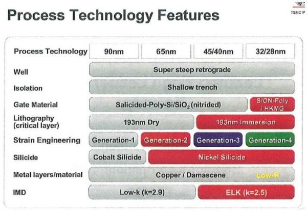
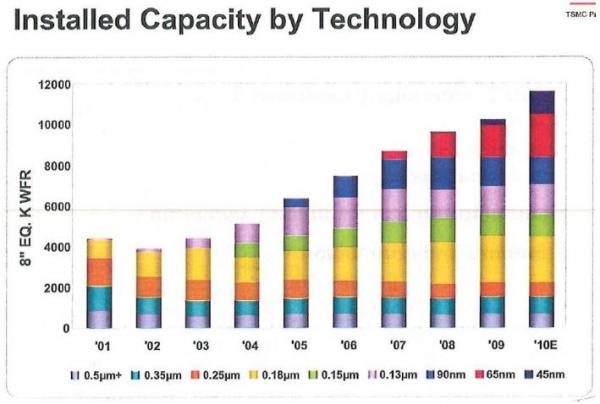
The new technologies introduced for the 45/40nm process include ArF immersion exposure, the third-generation strained silicon and a low-k interlayer insulating film whose dielectric constant was lowered to 2.5. Though TSMC had chamber matching and ion implanting problems for the 45/40nm process, it has solved the problems and is now rapidly ramping the technology. The number of tape-outs have increased at a rapid rate, and half of the taped-out chips are now being mass-produced, TSMC said.
The most important new technology for the 32/28nm process is a new gate. A SiON gate insulating film is used for the low-power type (28LP) while a high-dielectric gate insulating film and a metal gate electrode (high-k/metal gate) are used for the high-performance type (28HP) and the medium-speed, low-leakage type (28HPL).
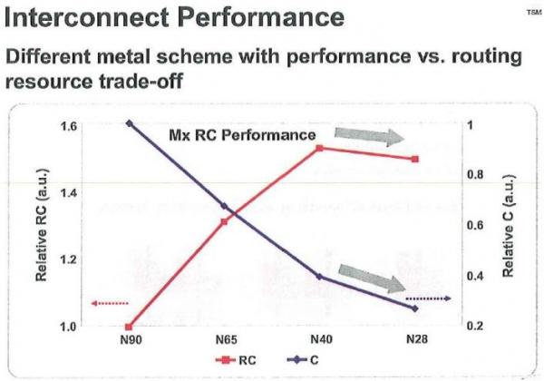
As a process to form the high-k/metal gate, TSMC employed the gate-gate-last process instead of the gate-first process, which the company was planning to use at first. Also, it will introduce the fourth-generation strained silicon and low-resistance Cu wiring. TSMC lowered the resistance of Cu wiring by improving the flatness of the boundary surfaces of the Cu and barrier metal to prevent electrons flowing on the surface of the wiring from scattering.
Besides TSMC, IBM and GLOBALFOUNDRIES have initiated research projects to enable the scaling of semiconductor components to the 22 nanometer node and beyond. Back in June 2009, GlobalFoundries described an innovative technology that could overcome one of the key hurdles to advancing high-k metal gate (HKMG) transistors, enabling the next generation of mobile devices with more computing power and improved battery life.
An interesting race indeed, the prize being the top foundry customers around the world: Qualcomm, Broadcom, Xilinx, Altera, AMD/ATI, Nvidia, Apple, etc…




Things From Intel 10K That Make You Go …. Hmmmm