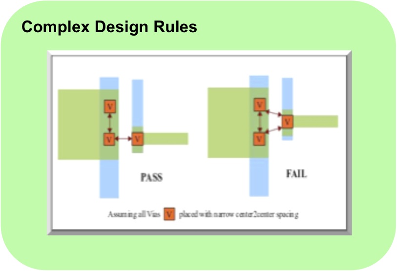
 The introduction of 28nm high-volume production for IC semiconductor devices will usher the era of “extreme low-k1” manufacturing, i.e. the unprecedented situation in the long history of the silicon technology roadmap, where computationally intensive (and EDA-driven) Design-Technology Co-Optimization will become the key enabler to a product success in terms of yield, time-to-market and profitability.
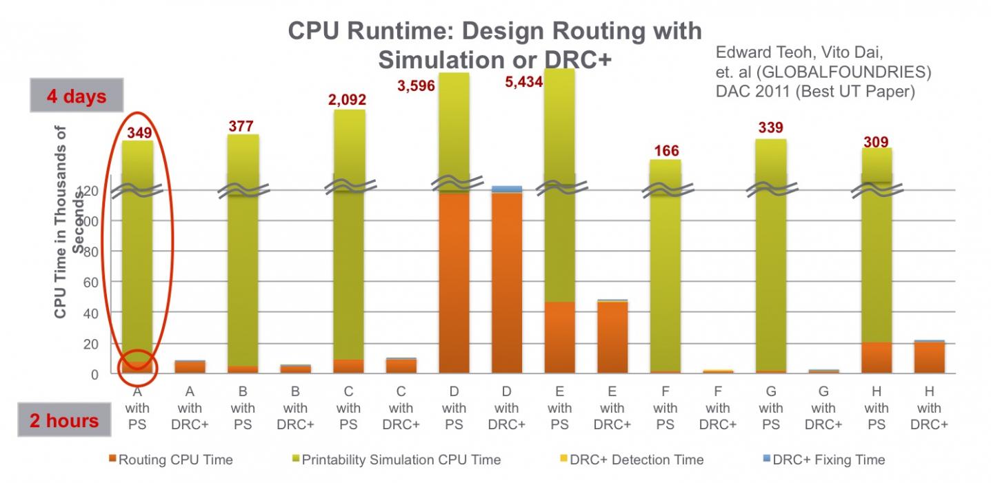
This talk will provide a review and technical analysis of the methodological innovations in Design Enablement flows which are being introduced for early production at 28nm, particularly advanced DFM physical verification and DFM-aware router implementations. Rule-based, model-based and the newly released pattern-matching based hybrid verification, pioneered, industry-first, at GLOBALFOUNDRIES are prominent examples of these new enablement flows.
 DFM methodologies are complemented by a set of novel foundry-based flows identified as Design-Enabled Manufacturing (DEM). While DFM provides process awareness into the design cycle through accurately calibrated models and verification flows (DFM sign-off), DEM enables manufacturing/design co-optimization, using automated physical design analysis and characterization, which in turn drive process optimization, fine-tuned to specific customer product designs.
The presentation will conclude with a preview of the “variability-challenge” intrinsic in the 20nm node and with an anticipation of the innovative EDA solutions which are currently being developed in the new Foundry-supported collaborative eco-system.
Luigi is a very engaging speaker on the leading edge of process technology, you definitely do not want to miss this one. See you there……
Register for this and other GLOBALFOUNDRIES Technical seminars @ DAC 2012 HERE.
BIOGRAPHY: Luigi Capodieci, Ph.D.
Director DFM/CAD – R&D Fellow – GLOBALFOUNDRIES
Dr. Luigi Capodieci has been working on lithographic imaging and process simulations for more than 15 years, with applications to Optical Proximity Correction, Phase Shift Masks, Resolution Enhancement Technology and Design/Process Co-Optimization.
At Advanced Micro Devices, in California, he pioneered the field of Design For Manufacturability (DFM) integrating physical design CAD flows with rigorous layout printability process modeling and novel verification algorithms.
He is currently an Engineering R&D Fellow and the Director of DFM/CADat GLOBALFOUNDRIES (www.globalfoundries.com), coordinating DFM R&D from 45 and 32/28nm, down to the next generations of 20 and 14nm technology nodes.
Dr. Capodieci holds a Doctor degree in Electronic Engineering and Computer Science from the University of Bologna, Italy and a Ph.D. in Electrical Engineering, from the University of Wisconsin-Madison, where he worked at the Center for Nanotechnology (CNTech, formerly Center for X-Ray Lithography).
Dr. Capodieci has authored and co-authored more than 35 journal and conference technical publications and is the principal inventor or co-inventor in more than 30 U.S. Patents. He is also an active member of the IEEE and ACM technical organizations.


Captain America: Can Elon Musk Save America’s Chip Manufacturing Industry?