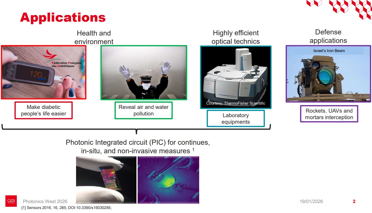


Mid-infrared (MIR) photonic integrated circuits are emerging as a key technology for applications ranging from environmental monitoring and medical diagnostics to defense and industrial process control. The MIR spectral region, often referred to as the molecular “fingerprint” region, exhibits strong absorption features for a wide variety of gases and chemical species. This property enables highly sensitive and selective sensing, provided that compact, efficient, and wavelength-stable laser sources can be integrated with photonic platforms. Among the available MIR sources, quantum cascade lasers (QCLs) stand out due to their broad wavelength coverage, high output power, and room-temperature operation. However, their integration on silicon remains a major technological challenge.
Quantum cascade lasers are unipolar semiconductor devices based on intersubband transitions in III-V heterostructures. Since their first demonstration in 1994, QCLs have undergone continuous improvements, achieving continuous-wave operation at room temperature and wall-plug efficiencies exceeding 20%. Despite these advances, most QCLs are still realized as discrete devices, limiting their scalability and integration with complex photonic systems. Silicon photonics, on the other hand, offers mature fabrication processes, high reproducibility, and large-scale integration capabilities, but silicon itself cannot provide optical gain in the MIR. Hybrid integration of III-V QCL gain regions onto silicon photonic platforms therefore represents a promising route toward compact and functional MIR photonic integrated circuits.

In this work, a high-index-contrast photonic integrated circuit platform is developed to enable the integration of III-V QCLs on silicon waveguides. The proposed architecture relies on molecular bonding of III-V epitaxial layers onto a silicon-on-insulator–based platform, including variants such as SONOI to extend MIR transparency. The platform combines several key functionalities: strong optical confinement for miniaturization, efficient and robust adiabatic coupling between the III-V gain region and silicon waveguides, and high-quality silicon-based distributed feedback structures for wavelength control. This approach enables the realization of distributed feedback (DFB) and distributed Bragg reflector (DBR) QCL architectures directly integrated with silicon photonic circuits.
Efficient optical coupling from the III-V active region into silicon waveguides is achieved using adiabatic tapers. Numerical studies show coupling efficiencies exceeding 95% over a wide range of taper lengths and geometrical parameters, demonstrating robustness against fabrication tolerances. This is a crucial requirement for wafer-scale fabrication and reproducible device performance. The silicon waveguides can further incorporate gratings or couplers for feedback, out-coupling, and on-chip routing toward sensing elements.
The fabrication process is fully compatible with 200-mm silicon wafers and includes silicon waveguide definition, dielectric deposition, III-V/Si molecular bonding, substrate removal, ridge and mesa etching, and metal contact formation. A usable surface ratio above 90% after III-V substrate removal highlights the maturity of the bonding approach. Laser characterization is performed at the wafer level using pulsed electrical injection, Peltier cooling, and automated probing, with optical output collected via grating couplers and analyzed using FTIR spectroscopy.
Experimental results demonstrate laser emission from hybrid DFB QCLs operating around 4.3 µm, a wavelength of particular interest for CO₂ detection. Clear lasing behavior is observed, with a threshold current of approximately 700 mA and a slope efficiency on the order of 0.22 mW/A under pulsed operation. Single-mode emission is achieved in the linear regime, while multimode behavior appears near rollover, mainly due to thermal limitations. These results confirm efficient light transfer from the III-V gain region into the silicon waveguide and validate the distributed feedback approach implemented in silicon.
Beyond DFB and DBR lasers, the platform also enables advanced diffractive and refractive architectures, such as photonic crystal surface-emitting lasers and micro-ring resonator-based QCLs. These concepts offer further reductions in footprint and threshold current, opening the way toward densely integrated MIR photonic systems. Overall, this work demonstrates a versatile and scalable hybrid III-V/silicon platform for quantum cascade lasers, representing a significant step toward fully integrated mid-infrared photonic circuits for sensing and beyond.
Also Read:
NanoIC Extends Its PDK Portfolio with First A14 Logic and eDRAM Memory PDK
TSMC’s 2026 AZ Exclusive Experience Day: Bridging Careers and Semiconductor Innovation
The Foundry Model Is Morphing — Again
Share this post via:


Silicon Insurance: Why eFPGA is Cheaper Than a Respin — and Why It Matters in the Intel 18A Era