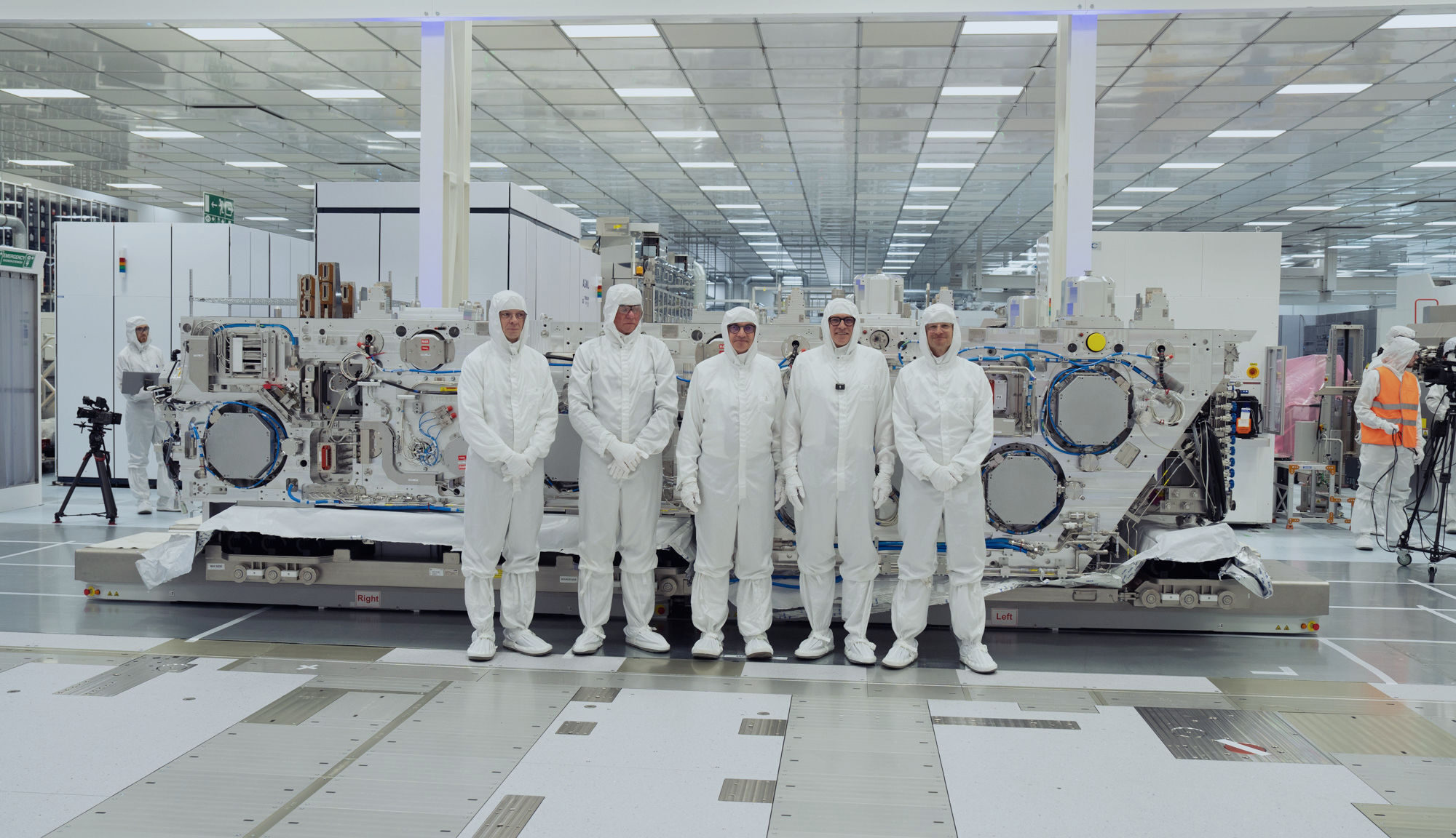


The imec installation of the ASML EXE:5200 High Numerical Aperture (High NA) extreme ultraviolet (EUV) lithography system at imec represents a pivotal advancement in semiconductor manufacturing and research. This system, installed in imec’s 300 mm cleanroom in Leuven, Belgium, introduces unprecedented lithographic resolution and process control required to enable sub-2 nm logic technologies and next-generation memory architectures. The integration of this High NA EUV platform with state-of-the-art metrology, patterning tools, and materials infrastructure is expected to accelerate learning cycles and support the scaling demands of AI and HPC applications.
High NA EUV lithography increases the numerical aperture from earlier EUV systems (0.33 NA) to approximately 0.55 NA, significantly improving optical resolution. This improvement allows smaller feature sizes to be printed in a single exposure, reducing reliance on multi-patterning techniques that add process complexity, cost, and variability. By delivering tighter pitch resolution and improved overlay accuracy, the EXE:5200 enables semiconductor manufacturers to extend Moore’s Law into the angstrom-scale era. Enhanced overlay performance is particularly critical for advanced transistor architectures such as GAA nanosheets and complementary CFET structures, where layer-to-layer alignment tolerances are extremely stringent.
The EXE:5200 system also introduces improvements in throughput and process stability. A redesigned wafer stocker and optimized stage mechanics reduce wafer handling variability, while improved illumination and projection optics enhance line-edge roughness and critical dimension uniformity. These capabilities are essential for ensuring high yield in advanced nodes. The system’s integration with advanced metrology equipment enables closed-loop process control, allowing rapid feedback between lithography, etch, and inspection steps. Such integration shortens process development timelines and allows imec and its partners to explore new patterning strategies at industry-relevant scales.
Imec’s collaborative ecosystem plays a crucial role in maximizing the value of High NA EUV technology. The research hub works closely with chip manufacturers, equipment vendors, resist suppliers, mask developers, and metrology experts. This ecosystem approach enables co-optimization of lithography processes, resist chemistry, mask design, and etch integration. For instance, resist materials must be engineered to balance sensitivity, resolution, and line-edge roughness under High NA exposure conditions. Similarly, mask 3D effects become more pronounced at higher numerical apertures, requiring advanced computational lithography and mask correction techniques. By providing early access to the EXE:5200, imec enables industry partners to collaboratively address these challenges and accelerate technology readiness.
Another important aspect of High NA EUV deployment is its impact on device scaling for AI and HPC workloads. As transistor densities increase, power efficiency and performance improvements are essential to support compute-intensive applications such as large-scale neural networks and data-center acceleration. Sub-2 nm technologies enabled by High NA EUV can deliver improved transistor switching speed, reduced leakage, and higher interconnect density. These advancements contribute to more efficient compute architectures, reduced latency, and improved energy efficiency in advanced processors. Furthermore, High NA EUV supports scaling of advanced memory technologies, including DRAM and emerging memory structures, which are critical for bandwidth-intensive AI systems.
The EXE:5200 installation is also strategically significant for regional semiconductor research leadership. As part of a broader partnership involving ASML, European initiatives, and national governments, the system strengthens Europe’s position in advanced semiconductor R&D. It forms a core component of imec’s pilot line infrastructure, enabling industry-relevant experimentation and technology transfer. The continued operation of the joint ASML-imec High NA EUV laboratory in Veldhoven ensures continuity in research activities during system qualification, which is anticipated to be completed by the fourth quarter of 2026.
Bottom line: the deployment of the ASML EXE:5200 High NA EUV lithography system marks a critical milestone in semiconductor scaling. By combining improved optical resolution, enhanced overlay control, higher throughput, and ecosystem collaboration, the platform enables exploration of angstrom-scale device architectures. This advancement supports continued innovation in logic and memory technologies, accelerates development for AI and HPC markets, and reinforces collaborative research frameworks necessary for next-generation semiconductor manufacturing.
Also Read:
Accelerating Computational Lithography Using Massively Parallel GPU Rasterizer
Unraveling Dose Reduction in Metal Oxide Resists via Post-Exposure Bake Environment
TSMC Process Simplification for Advanced Nodes
Share this post via:


Intel, Musk, and the Tweet That Launched a 1000 Ships on a Becalmed Sea