Recently, the statistics of secondary electron noise and its impact on defect probability in EUV lithography has been directly addressed for the first time[1]. In this article, we will take into account some updated blur models for EUV resists, both of the chemically amplified (CAR) and metal oxide (MOR) types.
First, let’s review the procedure of deriving the EUV stochastic defect probability, taking into account secondary electron noise. Photon absorption is characterized by the classical split or thinned Poisson distribution [2]. The number of electrons released per absorbed EUV photon is assumed to follow a uniform distribution of integers as the probability mass function [1]. When factoring in electron scattering, the resulting effective “blur” replaces the noisy photon absorption profile with a smoothed out profile characterized by the blur scale parameters.
However, this only updates the mean electron number per “pixel.” Here, the pixel represents the resist molecule size, which can be taken to be 2 nm x 2 nm for a CAR [3,4] and 1 nm x 1 nm for a MOR [4,5]. We can apply the cumulative distribution function (CDF) to predict whether the probability that the pixel is expected to be wrongly above or below the printing threshold. This CDF takes into account the blurred mean electron number in a pixel as well as the electron number noise. To calculate the probability of a defect of a given size at a given location, we simply calculate the product of such probabilities for the pixels within the defect region [1]. A natural consequence of this is that larger defects (containing more pixels) will have much smaller probabilities than smaller ones. This will be an important to bring up later as we consider the pitch dependence of defect probabilities.
The Significance of Resist Blur: Reduction of Contrast
Resist blur is essentially a resist response to light exposure, which causes the contrast to be degraded relative to the initial optical image. Chemically amplified resists are known to have blur resulting from acid diffusion [4], and EUV resists are known to have blur from electrons released by EUV photon absorption.
The acid blur function is generally a Gaussian shape [4]; the convolution with the pre-blur image forms the post-blur image.
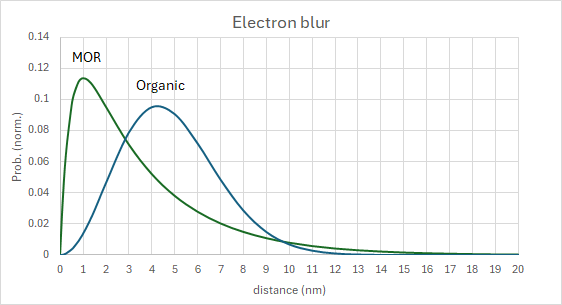
The electron blur impact is addressed similarly with the convolution treatment but the shape is realistically a difference of two functions, which allows a zero probability density at zero distance, but a peak probability density at a reasonable nonzero distance [6]. One of the functions (the “inner” function) has a shorter exponential decay length, which helps set the peak probability distance, while the other function (the “outer” function) has a longer exponential decay length which defines a long-range tail, corresponding to experimentally determined electron attenuation lengths [7,8].
Reducing the contrast means that all values are brought closer to the mean.
Electron blur actually includes distances traveled by electrons with energies starting from the photoelectron energy and going down to (nearly) zero. While the mean free path for an electron at a given energy may be on the order of 1 nm, the final electron blur tail decay length can easily be more than that.
Both forms of blur will reduce contrast to a degree which can be calculated for specific cases of interest. For example, a Gaussian shape with standard deviation s convolved with a sinusoidal wave of pitch p leads to contrast reduced by a factor of exp(-2*[pi*s/p]^2), while an exponential shape with scale parameter b convolved with the same sinusoidal wave leads to contrast reduced by a factor of 1/(1+[2*pi*b/p]^2). When taking the difference of two exponentials or Gaussians, the result must be divided by the difference of the relative weights of the functions, to re-normalize the result.
Reducing the contrast brings all pixel electron number (or acid number) values closer to the mean. Thus, the CDF calculation will give pixel probabilities closer to 50% as the contrast is reduced further. On the other hand, improved contrast means pixels further from the feature edge will have probabilities further reduced from 50%.
Updated Representative Resist Blur Models
Digging deeper into the literature, we can find some information that leads us to appropriate blur shapes for EUV resists. The electron blur shape for an EUV resist model based on PMMA was found by simulation of the degradation (chemical changes) resulting from EUV exposure [9]. The fit to their result is best achieved with a difference of Gaussians (one with s=3.4 nm, the other (relative weight 79.4%) with s=2.7 nm). Following convolution of this electron blur function with the photon absorption profile, an s=5nm Gaussian blur [4] is subsequently convolved with the result to get the acid profile to represent the CAR case. For the MOR case, we can refer to the data in Bespalov et al. [10], which shows a 1.6 eV electron penetrating 20 nm thick SnOH resist, then apparently reflected back from the substrate with dose-dependent degrees through the full thickness, and a 1.2 eV electron doing the same, but getting trapped ~11-12 nm from the top of the resist, when the electron kinetic energy reaches as low as the trap energy.
Note that if the electrons did not even reach the substrate, no resist thickness measurement would be possible, as the supporting bottom portion would have been dissolved. From an exponential fit, the 1.2 eV electron attenuation length is 1.4 nm, while the 1.6 eV electron attenuation length is 3.2 nm. Since all electrons must pass through 1.6 eV to get to the trapping energy, the outer blur scale parameter is taken to be the larger of the two (3.2 nm). The inner scale parameter (0.448 nm) and relative weight (14%) are chosen to meet the following two conditions: (1) zero probability at zero distance, and (2) a peak probability at 1 nm, matching the expected molecule size [5]. Figure 1 shows the electron blur function shapes resulting from the above treatment.

Representative Electron Noise Models for EUV Resists
Previously [1,11], electron noise was modeled as a uniform distribution over the integer range of 5 to 9 per photoelectron, i.e., absorbed photon. This allows for one electron to escape the Sn-based MOR layer. However, for the CAR case we will apply the same treatment to the result of Míguez et al in [9], modeling with an integer range of 8 to 16 per absorbed photon, including one escaped electron. As in [1], the minimum 3s/avg electron noise can be calculated for a range [p,q] as 3*sqrt([n^2-1]/12)/m, where m=(p+q)/2 and n=q-p+1. This gives 55% for the CAR case, and (as previously published [1]) 61% for the MOR case.
Using Pixel Probabilities with EUV Stochastics Effects
The probability that a pixel is defective is computed using Poisson CDFs averaged over each possible number of electrons per photon [1]. The CDF for the Poisson distribution for a given number of electrons per photon is commonly described in terms of the gamma function [12], and is basically the sum (for j=0 to k, the test absorbed photon or photoelectron number) of exp(-N)*Nj/j!, with N being the target or threshold absorbed photon or photoelectron number. For the case of CAR, the acid quantum yield (35%) is multiplied by the absorbed photon or photoelectron number. The effect of blur is to effectively bring the absorbed photon number at a given pixel close to the average (over all pixels), by scaling down the difference. The scale-down factor is the contrast reduction factor mentioned earlier in the context of the convolution of the absorbed photon profile with the blur profile.
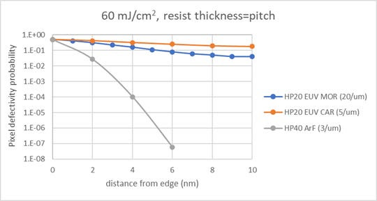
Pixel defectivity probabilities were calculated for three cases: (1) ArF immersion (ArFi) 40 nm half-pitch, 80 nm thick resist (3/um absorption), 2 nm pixel, s=5 nm Gaussian acid blur, (2) EUV 20 nm half-pitch, 40 nm thick CAR (5/um absorption), 2 nm pixel, s=5 nm Gaussian acid blur, (3) EUV 20 nm half-pitch, 40 nm thick MOR (20/um absorption), 1 nm pixel. The electron blur shapes for the EUV CAR and MOR were presented earlier (Figure 1). The results are shown in Figure 2.

Clearly, the EUV exposures are exponentially more defective throughout the 20 nm exposed half-pitch than the ArFi 40 nm half-pitch. This is why stochastic defectivity has become an apparent issue only with the arrival of EUV lithography.
Knowing the pixel probabilities allows one to calculate the probabilities for various EUV stochastics effects. However, interpretations of these probabilities must be formed with care.
Edge boundary pixels
The first thing to remember is that the edge pixel probability is always 50%. Since it represents the edge boundary of a feature, we can exclude it from consideration when assessing practical probabilities of stochastics effects.
Edge roughness
The line of pixels adjacent to the edge boundary pixels can be used to assess edge roughness. For an EUV incident dose of 60 mJ/cm2, there are 20-30 absorbed photons per pixel for both the CAR and MOR cases (5/um and 20/um absorption, respectively). The electron noise contribution is also comparable for both types of resists, with the larger average electrons/photon for CAR being compensated by a larger spread, compared to MOR. Thus, for both resists, the pixel probability is ~30-50% for the pixel adjacent to a 20 nm half-pitch edge boundary. The density of single defective pixels adjacent to the boundary can be found by dividing this probability by the practical tiling area of 40 nm pitch x (2 x pixel size). Equivalently, we can find the area per defect by reciprocating this density, giving roughly an occurrence of an edge defect every 2 pixels/30-50% = 4-6 pixels (8-12 nm for CAR, 4-6 nm for MOR). This is consistent with the ragged edges observed in previously published plots (e.g., [13]).
Edge Notch/Protrusion Defects
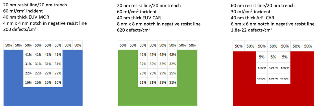
The pixel probabilities start at 50% at the edge and decrease moving away from it toward the interior of the feature. Hence, the most likely location for a defect to form as a result of Poisson noise + electron noise is at the edge. Consequently, an edge defect that extends several nm from the line edge and several nm along the line can have a high defect density, as shown in Figure 3. The tiling area used here to calculate defect density is pitch x (defect length + 1 pixel).

An ArF case is shown for reference, indicating how the defect density is exponentially lower, thanks to more photons absorbed in thicker resist, lacking the electron noise, and much less blur impact on a larger pitch. The larger pixel size of CAR (2 nm) compared to MOR (1 nm) is also disadvantageous, as an EUV CAR defect would have a worse defect density compared to a smaller MOR defect, as shown in Figure 3.
Line Breaks
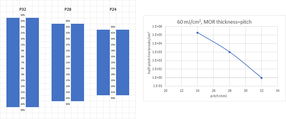
The probability of a line of defective pixels extending across a line depends crucially on the number of pixels that span the line. This number will of course be proportional to the linewidth, e.g., the half-pitch. This results in line break probabilities exponentially increasing as pitch decreases, as shown in Figure 4. The tiling area used here to calculate defect density is pitch x 2nm (i.e., defect width+ 1 pixel). Note that even with a defect density as high as 2e5/cm2, this corresponds to 524 um2/defect, i.e., it can’t be caught within one SEM picture.

When the pitch is reduced to 20 nm, wider line breaks can have large defect densities. A 2 nm wide line break in 20 nm thick MOR can have a defect density of 744/cm2. Here, the tiling area is 20 nm pitch x 3 nm (i.e., 2 nm width + 1 pixel).
Local Blur Variation
The possible local variation of blur was brought up previously [14,15]. This can have a big impact on defect density as well. Changing the outer electron blur scale parameter from 3.2 nm to 5 nm, while keeping zero probability at zero distance and a peak probability at 1 nm, leads to an increase in the density of the 4 nm x 4 nm edge defect of Figure 3 from 200/cm2 to over 1e5/cm2! Therefore, the actual defect density on the wafer depends on the relative probability of the 3.2 nm case vs. the 5 nm case on the wafer. This can be different for each different resist coating.
Optics Has Lost Control Over Lithography
As pitches shrink, it is no longer wavelength or NA, but resist blur, electron noise, and molecular size that have become the dominant factors in determining the practical resolution limit. In addition to image contrast and depth of focus, defect density has become the new consideration. That is why conventional projection lithography schemes will at some point have to rely on multipatterning [16].
Thanks for reading Exposing EUV! Subscribe for free to receive new posts and support my work.
References
[1] F. Chen, How Secondary Electrons Worsen EUV Stochastics.
[2] K. Siegrist, Thinning and Superposition.
[3] M. M. Sung et al., “Vertically tailored hybrid multilayer EUV photoresist with vertical molecular wire structure,” Proc. SPIE PC12953, PC129530K (2024).
[4] H. Fukuda, “Statistics of EUV exposed nanopatterns: Photons to molecular dissolutions,” J. Appl. Phys. 137, 204902 (2025).
[5] R. Maas et al., “Stochastics in extreme ultraviolet lithography: investigating the role of microscopic resist properties for metal-oxide-based resists,” J. Micro/Nanolith. MEMS MOEMS 17, 041003 (2018).
[6] F. Chen, A Realistic Electron Blur Function Shape for EUV Resist Modeling.
[7] O. Kostko, M. Mueller, and P. Naulleau, “Evaluation of Electron Blur for Different Electron Energies,” J. Photopolymer Sci. and Tech. 37, 315 (2024).
[8] M. I. Jacobs et al., “Low energy electron attenuation lengths in core–shell nanoparticles,” Phys. Chem. Chem. Phys. 19, 13372 (2017).
[9] L. F. Míguez, P. A. Bobbert, and R. Coehoorn, “Towards molecular-scale kinetic Monte Carlo simulation of pattern formation in photoresist materials for EUV nanolithography,” Proc. SPIE 12498, 124980E (2023).
[10] I. Bespalov et al., “Key Role of Very Low Energy Electrons in Tin-Based Molecular Resists for Extreme Ultraviolet Nanolithography,” ACS Appl. Mater. Interfaces, 12, 9881–9889 (2020).
[11] F. Chen, Impact of Varying Electron Blur and Yield on Stochastic Fluctuations in EUV Resist.
[12] https://en.wikipedia.org/wiki/Poisson_distribution.
[13] F. Chen, Facing the Quantum Nature of EUV Lithography.
[14] F. Chen, Modeling EUV Stochastic Defects with Secondary Electron Blur.
[15] F. Chen, Measuring Local EUV Resist Blur with Machine Learning.
[16] F. Chen, Multiple Patterns.
This article first appeared in Exposing EUV: Predicting Stochastic EUV Defect Density with Electron Noise and Resist Blur Models
Also Read:
How Secondary Electrons Worsen EUV Stochastics
Via Multipatterning Regardless of Wavelength as High-NA EUV Lithography Becomes Too Stochastic
EUV Lithography Without Pellicles: Accounting for Low Yields
Share this post via:


Quantum Computing Technologies and Challenges