Embedded memory makes computing applications run faster. In the early days of the semiconductor industry, the desire to utilize large amount of on-chip memory was limited by cost, manufacturing difficulties and technology mismatches between logic and memory circuit implementations. Since then, advancements in semiconductor manufacturing have been bringing on-chip memory costs down.
Fast forward to today, applications such as AI, machine learning, mobile and other low-power applications have been fueling demands for large amounts of embedded memories. A challenge with SRAM-based memory processing elements is that they consume a lot of power which is not affordable by many of the above mentioned applications. In addition, many of the existing embedded non-volatile memory (NVM) technologies such as flash face challenges as the process node goes below 28nm. The challenges are due to additional material layers and masks, supply voltages, speed, read & write granularity and area.
Resistive RAM (ReRAM or RRAM) is a promising technology that is specifically designed to work in finer geometry process nodes where charge-based NVM technologies face challenges. It is true that ReRAM as a technology has spent many decades in the research phase. For satisfying NVM needs, Flash technology had the edge for many applications until 28nm.
ReRAM’s simplicity for process manufacturing makes it easier to be integrated into Back End of Line (BEOL) with only a few extra masks and steps. ReRAM technology enables high-speed, low-power write operations and increased storage density, all critical for AI computing-in-memory applications, as an example.
At the IP-SoC Conference 2022, Eran Briman of Weebit Nano talked about their ReRAM offering and how a wide range of markets and applications could benefit from it.
Who is Weebit Nano?
Weebit Nano is a leading developer of ReRAM technology based IP. They license their IP to FSCs and Fabs to manufacture the chips embedding this IP. From their early days in 2015, Weebit Nano has strategically partnered with CEA-Leti to leverage research in NVM and specifically on ReRAM.
Weebit Nano’s ReRAM Technology
Weebit Nano’s ReRAM technology is based on the creation of a filament that is made of oxygen vacancies in a dielectric material, and is hence called OxRAM. The dielectric layer is deposited between 2 metal stacks at the BEOL, and by applying different voltage levels a filament is either created, representing a logical 1, or dissolved, representing a logical 0. The technology is inherently resistant to tough environmental conditions as the information is retained within the stack itself. As a result, OxRAM is resilient in its operation at high temperatures, exposure to radiation and EM fields. The technology also utilizes materials and tools commonly used in standard CMOS fabs.
The resulting Weebit Nano based NVM solution is also very cost-effective as it requires only two additional masks compared to around 10 additional masks for embedded Flash. It is also power efficient as programming can be done at below 2V compared to at around 10V for embedded Flash. During operation, memory reads can be accomplished at 0.2V which is very power efficient.
Weebit ReRAM Status/Availability
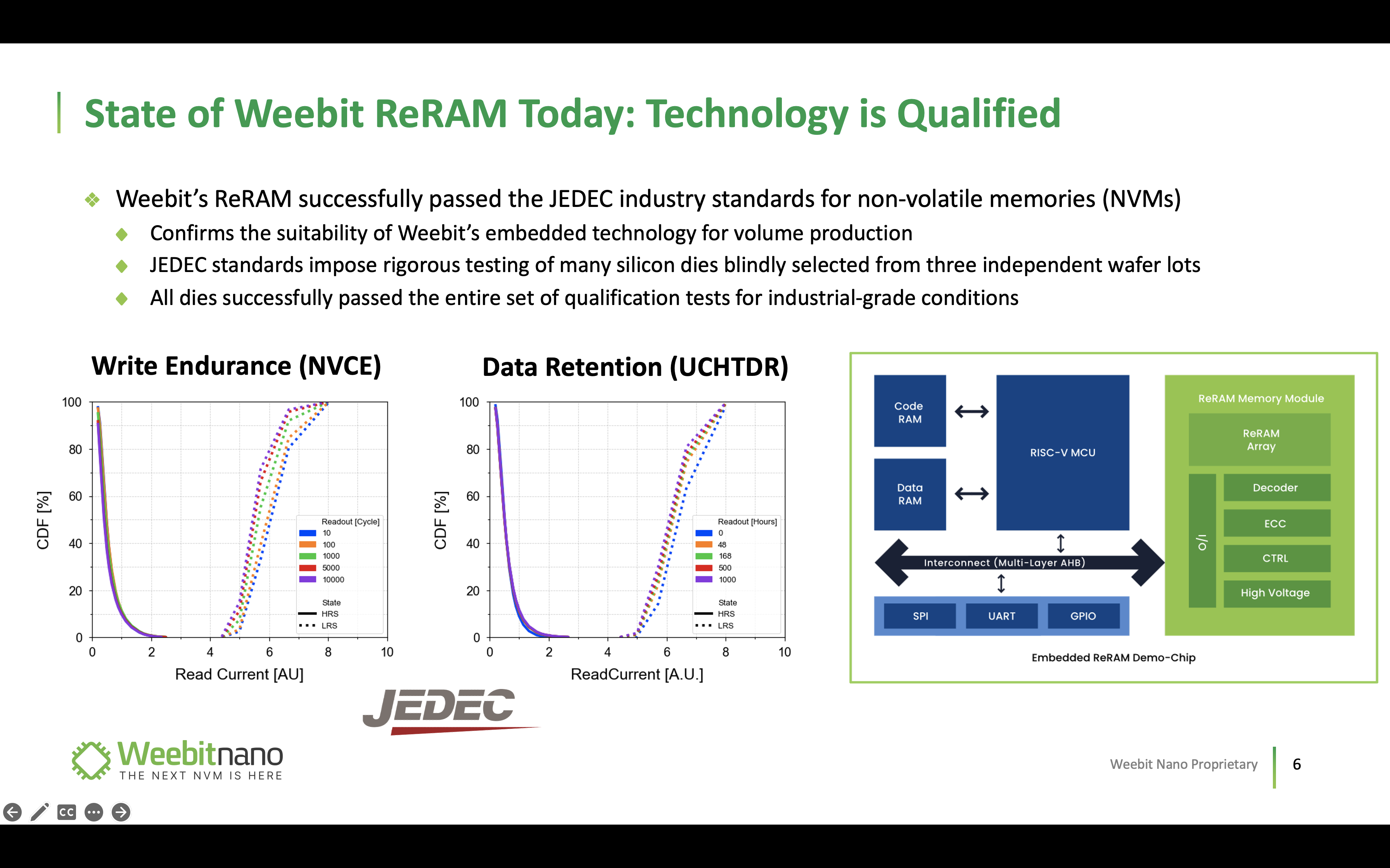
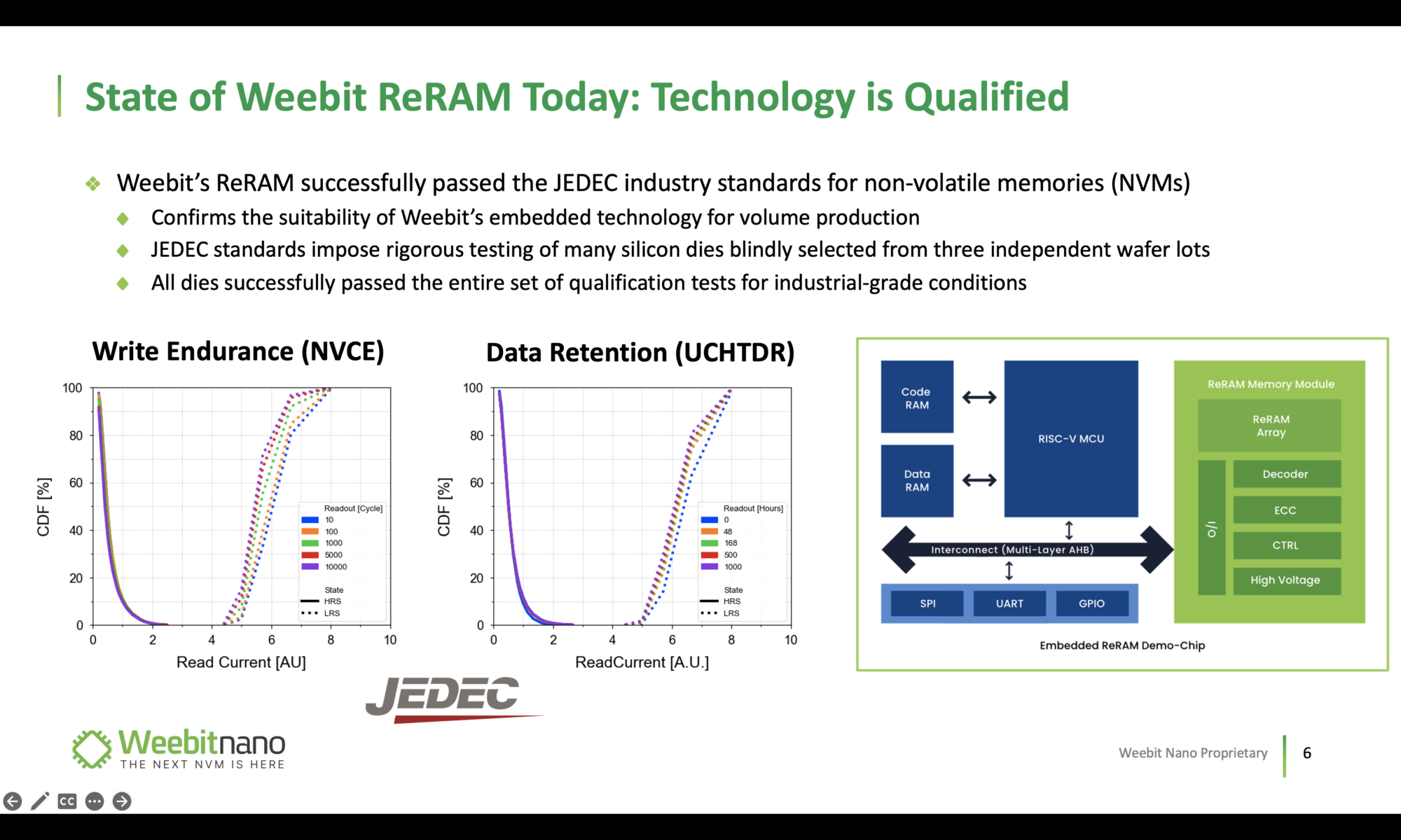
The technology is now production ready as of November 2022, with wafers having been manufactured in 130nm to 28nm to date. Getting to production ready status required passing JEDEC industry standard qualification process for NVM memories. The qualification process includes rigorous tests for endurance, retention, retention of cycling, solder reflows, etc., on hundreds of blindly selected dies from three independent wafer lots.

Weebit Nano’s first production manufacturing partner SkyWater recently produced 130nm wafers embedding Weebit’s 256Kb ReRAM module. The dies are now going through the JEDEC qualification process and are available for customers to integrate into a range of target SoCs.
ReRAM: Why Now?
As noted earlier, Flash memory is facing scaling limitations beyond 28nm along cost and complexity dimensions. At the same time, the pressure for lower power and lower cost solutions is increasing, pushing products toward more advanced process nodes. ReRAM technology scales nicely beyond 28nm and fits easily in bulk CMOS, FD-SOI as well as FinFET processes. It can also support low power, high performance, RF CMOS, high-voltage and other process variants too. This opens up target markets to include mixed-signal, power management, MCUs, Edge AI, Automotive, Industrial and Aerospace & Defense applications. According to Yole, a market research firm, the embedded ReRAM market is projected to grow from less than $20M in 2021 to around $1B in 2027.
Why Weebit Nano ReRAM?
Refer to the following table which highlights how Weebit Nano’s ReRAM IP addresses key requirements of various applications in fast growing markets.

Those looking into designing chip solutions for applications that could benefit from embedded memories should reach out to Weebit Nano to get more insights about their ReRAM solutions.
Share this post via:


Comments
One Reply to “How an Embedded Non-Volatile Memory Can Be a Differentiator”
You must register or log in to view/post comments.