In today’s rapidly evolving semiconductor industry, the design and integration of intellectual property (IP) play a pivotal role in achieving competitive advantage and market success. Whether sourced from commercial IP providers or developed in-house, ensuring that IP designs are compliant with signoff requirements and seamlessly integrable into larger designs is paramount. From managing design complexity to ensuring power efficiency and security, IP designers must navigate a multitude of factors while striving to meet tight deadlines and maintain quality standards. Additionally, the rise of third-party IP usage and design reuse further complicates the landscape, necessitating interoperability and compatibility across different IP blocks and design modules. The complexity and competitiveness of the IP design landscape necessitate efficient verification processes that minimize time-to-market and resource requirements. Siemens EDA addresses this topic in-depth in a recently published technical whitepaper.
The Importance of Early Verification
Commercial IP design is a fiercely competitive arena, while in-house IP development offers the opportunity for design companies to differentiate themselves by incorporating innovative functionality into their integrated circuit (IC) designs. Regardless of the source, ensuring that IP designs are signoff-compliant and ready for integration into larger designs is essential for maintaining a competitive edge. In addition, Block/chip designers and designers working on three-dimensional integrated circuits (3DICs) also encounter unique verification challenges that require specialized solutions. Reducing the time and resources required for design, implementation, and verification directly impacts marketability and profitability.
One of the key strategies for streamlining the IP design process is the early detection and correction of physical verification issues. By identifying and addressing these issues in the initial stages of the design process, designers can minimize the risk of costly errors and delays during later stages.
Siemens EDA’s Calibre Shift Left Solutions
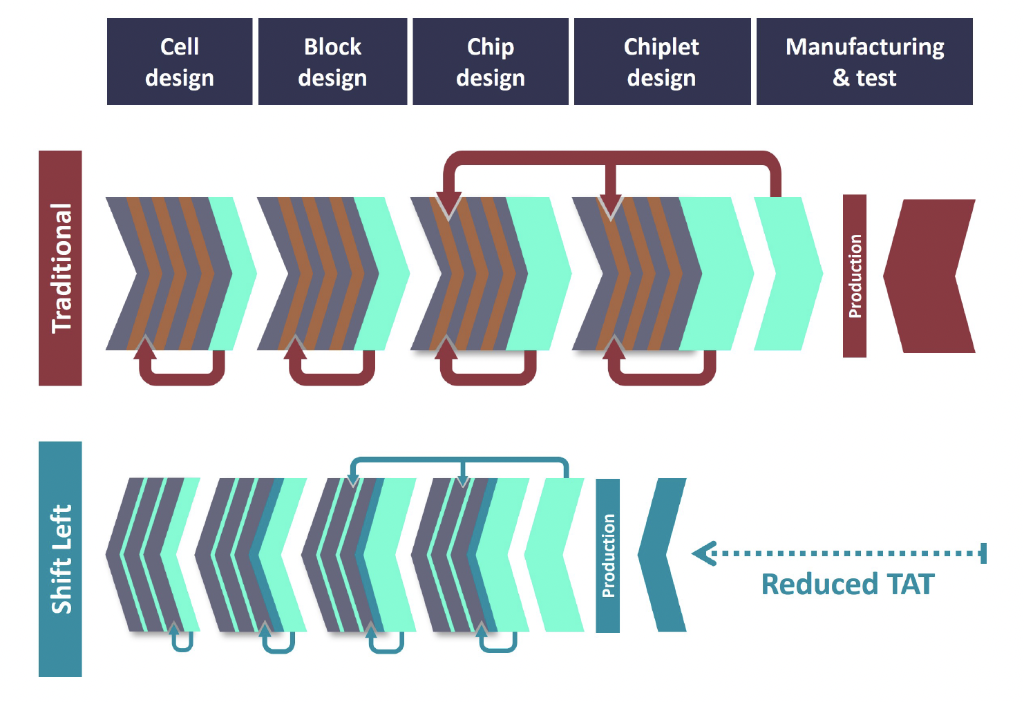
Calibre Shift Left solutions provide a comprehensive approach to streamlining the IP design process. These solutions combine proven Calibre technology with innovative strategies to support consistent and thorough verification of IP designs while maximizing productivity and efficiency. By shifting select physical verification and design optimization tasks earlier in the design and implementation workflows, Calibre Shift Left solutions empower design teams to accelerate time-to-market and achieve volume production faster.

Calibre Shift Left Solutions Enable Enhanced Productivity and Reduced Time to Market
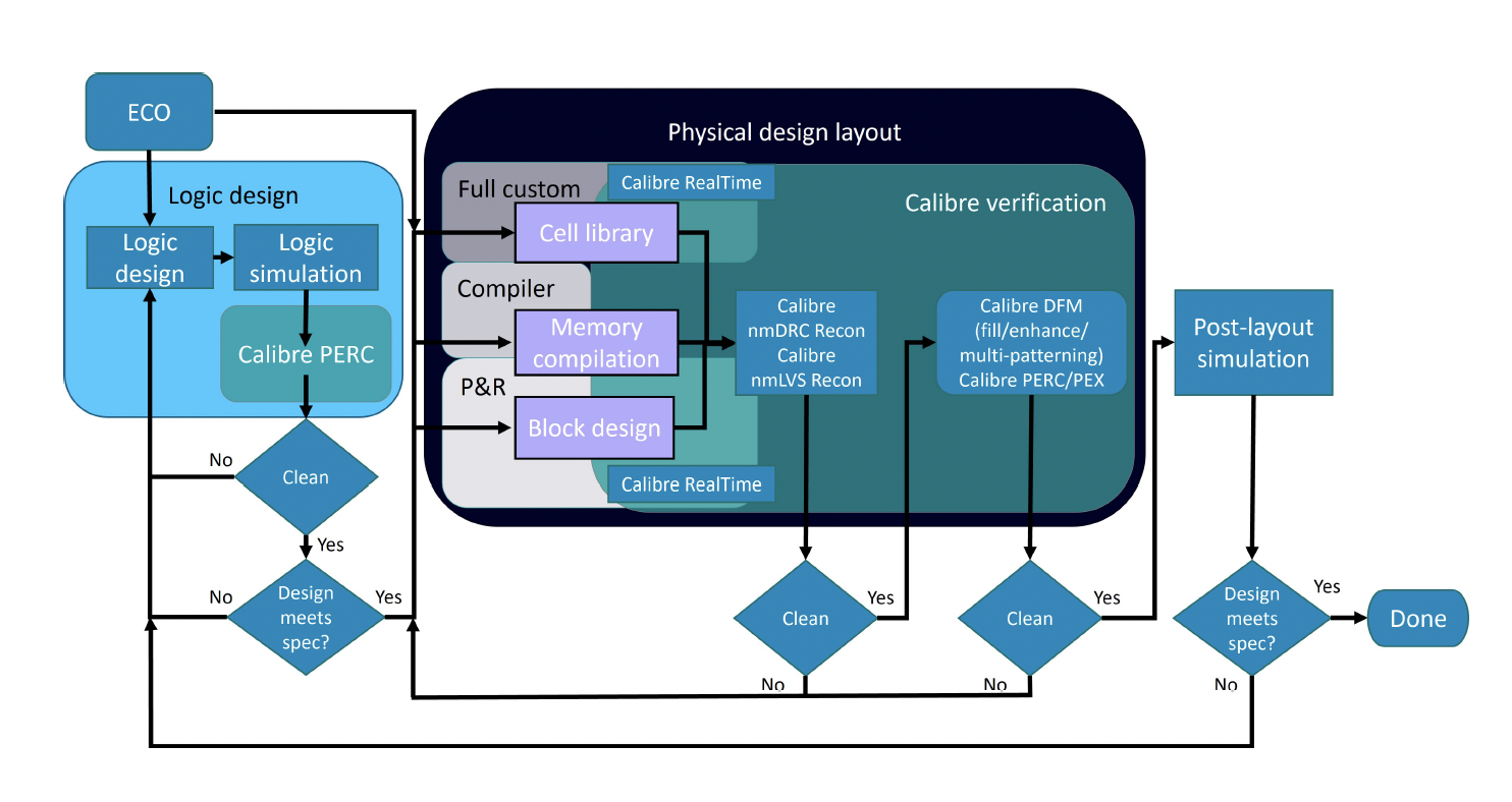
From early detection of design issues to comprehensive verification of IP designs, Calibre Shift Left solutions provide the flexibility and scalability needed to meet the diverse needs of semiconductor design teams. Calibre Shift Left solutions offer advanced tools and methodologies to facilitate early detection of physical verification issues, enabling designers to proactively address these challenges and ensure compliance with signoff requirements.

Shift Left Physical Verification in IP Design Flows
Prioritizing and Categorizing Design Issues
Efficient resolution of design issues is essential for maintaining productivity and meeting project deadlines. Prioritizing and categorizing design issues allows designers to focus their efforts on resolving critical issues first, minimizing time and resource wastage. Calibre Shift Left solutions provide functionalities to prioritize and categorize design issues, enabling designers to allocate resources effectively and accelerate the resolution process.
Tailored Benefits for Different IP Design Types
Calibre Shift Left solutions offer specific advantages tailored to different IP design types. For hard IP designers, early verification enables rapid identification and resolution of modified IP components, minimizing retesting requirements and ensuring smooth integration into larger designs. Soft IP designers benefit from early SRAM IP integrity validation, mitigating compilation issues before finalizing the design. Custom IP designers can leverage tools like Calibre RealTime Custom and Calibre Pattern Matching to streamline verification processes and reduce runtime and debug cycles.
Aligning IP Cell Verification with Larger Chip Designs
Ensuring consistency and alignment between IP cell verification and larger chip designs is crucial for seamless integration and optimal performance. Calibre Shift Left solutions enable designers to align IP cell verification with the same intent as larger chip designs, ensuring compatibility and interoperability across different design components. By leveraging Calibre’s proven technology, designers can streamline the verification process and minimize discrepancies between IP cells and larger chip designs.
Extending Beyond IP Design
Beyond IP design, block/chip designers and 3DIC designers can also benefit from Calibre Shift Left solutions to address their unique verification challenges. These solutions enable designers to apply early verification stages efficiently within familiar environments, ensuring high-quality results while accelerating the design process. Calibre Shift Left solutions not only optimize resource utilization but also enhance design agility and competitiveness in today’s dynamic semiconductor landscape.
Optimizing Performance and Automation
Performance optimization and automation play a crucial role in enhancing the efficiency of early design-stage verification. Calibre Shift Left solutions offer advanced optimization techniques and automation capabilities to minimize runtimes and maximize resource efficiency. By integrating Calibre tools into design and implementation environments, designers can streamline verification processes and accelerate design closure while ensuring signoff-quality results.
Summary
In a competitive semiconductor landscape, the Calibre Shift Left solution emerges as a game changer for streamlining the IP design process and enhancing overall efficiency. By addressing key challenges such as early detection of physical verification issues, efficient resolution of design issues, and alignment of IP cell verification with larger chip designs, Calibre Shift Left solutions empower designers to deliver high-quality IP designs in a timely manner. By streamlining verification processes, minimizing time-to-market, and optimizing resource utilization, Calibre Shift Left solutions allow companies to stay ahead of the curve.
Siemens EDA’s whitepaper titled “A game-changer for IP designers: design-stage verification” is essential reading for designers, engineers, and engineering managers aiming to streamline and enhance the efficiency and accuracy of their design processes.
Also Read:
AI and SPICE Circuit Simulation Applications
Mastering Mixed-Signal Verification with Siemens Symphony Platform
Cryogenic Semiconductor Designs for Quantum Computing
Share this post via:


Comments
There are no comments yet.
You must register or log in to view/post comments.