As we all know, the age of multi-die design has arrived. And along with it many new design challenges. There is a lot of material discussing the obstacles to achieve more mainstream access to this design architecture, and some good strategies to conquer those obstacles. Synopsys recently published a webinar that took this discussion to the next level. The webinar began with an overview of multi-die design and its challenges, but then an Intel technologist weighed in on what he’s seeing and how the company is collaborating with Synopsys.
The experience of a real designer is quite valuable when discussing new methodologies such as multi-die design and this webinar provides that perspective. There are great insights to be gained. A replay link is coming but first let’s take a big picture view of this Synopsys webinar – enabling multi-die design with Intel.
The Synopsys Introduction

The webinar begins with a short but comprehensive context setting from Amlendu Shekhar Choubey, Senior Director, Product Management at Synopsys. He manages the 3DIC Compiler platform and has over 20 years of experience in EDA, semiconductor IP, and advanced packaging, with a strong background in product management, product strategy, and strategic partnerships. Amlendu has expertise in package-board software, including AI-driven design solutions, cloud-based services, and driving growth in emerging markets. He holds an MBA from UC Berkeley’s Haas School of Business and a B. Tech in Electrical Engineering from IIT Kanpur.
Amlendu began with an eye-catching chart depicting the impact AI has had on the size of the semiconductor market. Another sobering prediction is that 100% of Al chips for data centers will be multi-die designs. The chart is shown below.

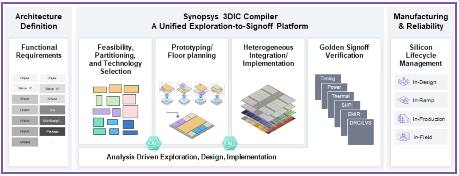
He concluded his presentation and set the stage for what followed with an overview of the Synopsys multi-die design solution, focusing more on Synopsys 3DIC Compiler exploration-to-signoff paltform. The goal of this approach is to efficiently create, implement, optimize, and close in one place. The platform is depicted in the chart below.

Now, let’s look at some brief highlights of comments from Intel.
Intel Presents: Modern EDA Solutions for Scalable Heterogeneous Systems

This portion of the webinar was presented by Vivek Rajan, Senior Principal Engineer at Intel. Vivek has over 25 years of experience in digital design methodology, chip integration, technology, and 3DIC system co-optimization. Vivek received his bachelor’s degree in electrical engineering from IIT Kharagpur, India and his master’s degree in electrical systems engineering from University of Connecticut. Vivek actively raises awareness and drives innovation for emerging shifts in chip Integration and systems design. As an invited speaker, Vivek has delivered several technical presentations at industry conferences.
Vivek began by saying that, “It is a great pleasure to present this webinar on multi-die challenges and opportunities … and what we have done collaborating with Synopsys for many years.” Vivek’s presentation outline includes:
- Executive Summary
- Multi-Die Challenges and Opportunities
- Generational Collaboration Between Intel and Synopsys for Multi-Die Solutions
- Peeking Ahead: Core Folding
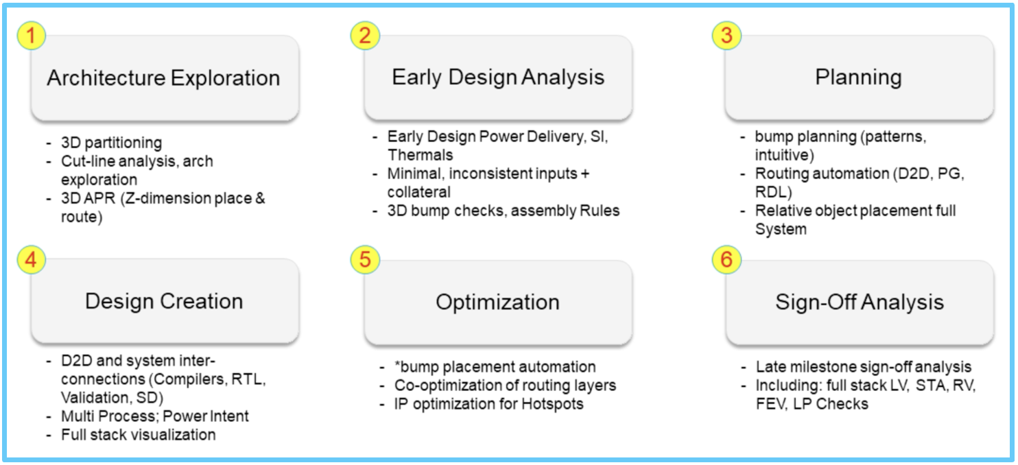
Vivek discussed some of the unique challenges of managing and configuring die-to-die IP and how Intel has approached this challenge. He then goes into substantial detail on the many planning requirements for 3D IC design. He discusses the many focus areas of collaboration between Intel and Synopsys which are summarized below.

The details of the 3D IC planning and implementation workflows being developed at Intel are presented. Vivek also goes into detail regarding core folding, an approach to partitioning and layout of 3D designs.
He concludes with the following points:
- EDA tool capabilities are essential enablers for Multi Die Designs
- Our (INTC/SNPS) collaboration has been fruitful for Intel & ecosystem!
- Early Design Prototype enablement is paramount for decision making
- Today, tool features for 3DIC Construction & assembly are fully available
- Next step is full automation for Core Folding and Scale
To Learn More
A webinar that highlights a real designer’s perspectives and experiences is quite valuable. If multi-die design is in your future, seeing what Intel is doing can be quite useful.
You can access the webinar here: Intel Presents: Modern EDA Solutions for Scalable Heterogeneous Systems. And that’s the Synopsys webinar – enabling multi-die design with Intel.
Also Read:
cHBM for AI: Capabilities, Challenges, and Opportunities
Share this post via:


Comments
There are no comments yet.
You must register or log in to view/post comments.