IEDM was buzzing with many presentations about the newest gate-all-around transistor. Both Intel and TSMC announced processes based on nanosheet technology. This significant process innovation allows the fabrication of silicon RibbonFET CMOS devices, which promise to open a new era of transistor scaling, keeping Moore’s Law alive. It seems fitting that Intel should be leading this charge and the company’s innovation was on display at IEDM. The company presented “Silicon RibbonFET CMOS at 6nm Gate Length”. A summary of these results are shown in the graphic above. This technology was referred to as the last innovation for current transistor design. So, let’s examine how Intel presents the final frontier in transistor architecture at IEDM.
The Presenter

The work presented was a collaboration of many folks from Intel Foundry Technology Research and Intel Foundry Technology Development, both in Hillsboro, Oregon. The presentation was given by Dr. Ashish Agrawal, senior device engineer.
Ashish has been with Intel for over 10 years. His areas of focus include R&D in semiconductor front-end materials and physics, electrical characterization using his background in device physics and material science and design-technology co-optimization (DTCO). The DTCO work includes analysis of novel materials, devices, and architectures for future scaled technology nodes.
Ashish presented a lot of results for this new transistor architecture. Let’s examine some of what was presented.
Some Results
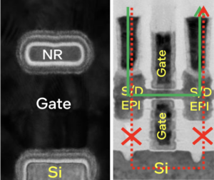
To accurately characterize true behavior of the RibbonFET at extreme gate length scaling, a novel, single nanoribbon (1NR) flow was developed in which source/drain are disconnected from the subfin. This ensures accurate knowledge of transistor dimension data and precise probing of NR characteristics.

A TEM micrograph the device is shown to the right. With Si/SiGe Epi stack innovation, the subfin is disconnected successfully from S/D epi in addition to healthy and uniform inner spacer above and below the NR.
Ashish explained that gate length scaling below 10nm was achieved by innovation in gate lithography and a dummy polysilicon etch process. He went on to say that source drain junctions and their doping profiles carry a new meaning and new implications at the small gate lengths being used in this work. Intel has done substantial work on the source/drain junctions to optimize for engineered short-channel effects and achieve the best performance possible from this highly scaled device.
Ashish also pointed out that, at a 6nm gate length you don’t have enough room to put in Hi-K, and di-pole and a work function to achieve the Vt target. So, for this technology, a work function was optimized and engineered to achieve a low Vt close to the target. Process innovation was critical to achieve effective scaling below a 10nm gate length.
As the gate length is scaled below 10nm, the source/drain doping profile in the tip region needs to be carefully examined. Highly diffused junctions not only degrade short channel effects but also result in remnant doping in the channel which degrades performance due to poor mobility from ionized impurity scattering. In the figure below, (a) shows peak Gmlin for LG=18nm and LG=100nm, highlighting a 34% gain in Gmlin with optimized junction Process B at short LG whereas long LG transconductance is matched. (b) shows drain induced barrier lowering (DIBL) vs. process indicating improved short channel effects with an optimized Process B junction profile. (c) shows Rext vs. process showing matched Rext for both processes and a very low value indicating no penalty from junction optimization.

Ashish presented many more results that demonstrated effective scaling all the way down to a gate length of 6nm and nanoribbon thickness of 1.5nm. He concluded by saying that this work paves the path for continued gate length scaling, which is a cornerstone of Moore’s Law. And that’s how Intel presents the final frontier in transistor architecture at IEDM.
Also Read:
Intel – Everyone’s Favourite Second Source?
Share this post via:


Comments
There are no comments yet.
You must register or log in to view/post comments.