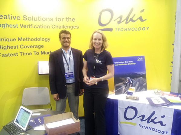
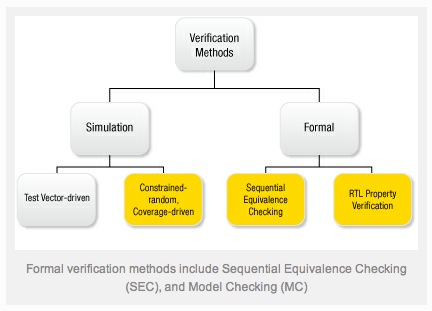
Most of what you see at DAC is canned PowerPoint presentations, however on Tuesday afternoon I spotted a company called Oski Technology that was doing something almost unheard of – they had an engineer debugging a digital design from Nvidia using formal tools live. I later found out the engineer found 4 bugs in just three days without any assistance from Nvidia.

From UC Berkeley, named after the bear mascot.
Sunday at 5PM Nvidia gave Oski a blind design from a mobile design, 45K FF’s, mature design.
Goal – find bugs, formally verify 4 out of 6 stages, not analyze and measure for this 72 hour challenge. After 48 hours already found one bug (Live twitter feed #OskiTech). Specs were out of date, got the new specs with correct signal names.

Founded in 2005, also founded Jasper.
ALready are some assertions in the design, however with Oski they are creatin their own constraints, reference model and checkers. Design intent is needed, just about 10 minutes. Some waveforms provided, then infer the operation at a high level.
White box verification.
Vigyan Shihai, President and CEO.
News – live challenge on an unknown design. Don’t sell tools, rather sell consulting service with a team of 20 people located in Bay Area and New Dehli.
Using Cadence IEV tools, with the Oski methodlogy which is tool agnostic.
How do you charge for consulting? Per bug like Nvidia. Hire like an insurance policy. Create a Statement of work.
Customers: CIsco, XIlinx, CYpress Semi, Synopsys IP group, Nvidia.
Services company.
Contact company in Mtn View to start an engagement. Team training available as well. Take a real design and work with team to bring them up to speed. Big three EDA companies send consulting business to Oski. Joined the 3rd party programs: OneSpin, Mentor, Cadence, Synopsys.

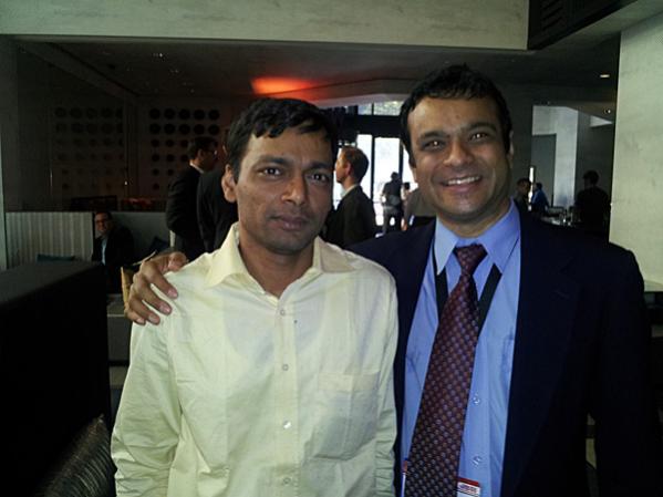
Engineer in Yellow shirt from Oski that found the four RTL bugs


Intel, Musk, and the Tweet That Launched a 1000 Ships on a Becalmed Sea