- This event has passed.
Advanced CMOS/FinFET Fabrication
February 19 - February 20

Semiconductor and integrated circuit developments continue to proceed at an incredible pace. For example, today’s microprocessor chips have one thousand times the processing power of those a decade ago. These challenges have been accomplished because of the integrated circuit industry’s ability to track something known as Moore’s Law. Moore’s Law states that an integrated circuit’s processing power will double every two years. This has been accomplished by making devices smaller and smaller. The question looming in everyone’s mind is “How far into the future can this continue?” Advanced CMOS/FinFET Fabrication is a 2-day course that offers detailed instruction on the processing used in a modern integrated circuit, and the processing technologies required to make them. We place special emphasis on current issues related to manufacturing the next generation devices. This course is a must for every manager, engineer and technician working in the semiconductor industry, using semiconductor components or supplying tools to the industry.
By concentrating on the latest developments in CMOS and FinFET technology, participants will learn why FinFETs are fast becoming the technologies of choice at feature sizes below 20nm. Our instructors work hard to explain semiconductor processing without delving heavily into the complex physics and materials science that normally accompany this discipline.
What Will I Learn By Taking This Class?
Participants will learn basic, but powerful, aspects about CMOS fabrication and FinFET technology. This skill-building series is divided into four segments:
- Front End Of Line (FEOL) Overview. Participants will study the major developments associated with FEOL processing, including Ion Implantation, Rapid Thermal Annealing (RTA) for implants and silicides, and Pulsed Plasma Doping. They will also study alternate substrate technologies like SOI, as well as High-k/Metal Gates for improved leakage control.
- Back End Of Line (BEOL) Overview. Participants will study the major developments associated with BEOL processing, including copper metallization and Low-k Dielectrics. They will learn about why they’re necessary for improved performance.
- FinFET Manufacturing Overview. Participants will learn how semiconductor manufacturers are currently processing FinFET devices and the difficulties associated with three-dimensional structures from a processing and metrology standpoint.
- FinFET Reliability. Participants will study the failure mechanisms and techniques used for studying the reliability of these devices.
Course Objectives
- This course will provide participants with an in-depth understanding of Bulk technology, SOI technology and the technical issues.
- Participants will understand how Hi-K/Metal Gate devices are manufactured.
- Participants will also understand how FinFET devices are manufactured.
- This course will provide a look into the latest challenges with copper metallization and Low-k dielectrics.
- Participants will understand the difficulties associated with non-planar structures and methods to alleviate the problems.
- Participants will be able to make decisions about how to evaluate FinFET devices and what changes are likely to emerge in the coming years.
- Participants will briefly learn about IC reliability and the failure modes associated with these devices.
- Participants will see a comparison between FinFETs and new alternatives (such as Gate All Around (GAA) structures and nanosheets).
Instructional Strategy
By using a combination of instruction by lecture, classroom exercises, and question/answer sessions, participants will learn practical information on semiconductor processing and the operation of this industry. From the very first moments of the seminar until the last sentence of the training, the driving instructional factor is application. We use instructors who are internationally recognized experts in their fields that have years of experience (both current and relevant) in this field. The accompanying textbook offers hundreds of pages of additional reference material participants can use back at their daily activities.
Instructor Profile
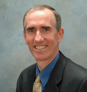
Christopher Henderson, President of Semitracks

Christopher Henderson received his B.S. in Physics from the New Mexico Institute of Mining and Technology and his M.S.E.E. from the University of New Mexico. Chris is the President and one of the founders of Semitracks Inc., a United States-based company that provides education and semiconductor training to the electronics industry.
From 1988 to 2004, Chris worked at Sandia National Laboratories, where he was a Principal Member of Technical Staff in the Failure Analysis Department and Microsystems Partnerships Department. His job responsibilities have included failure and yield analysis of components fabricated at Sandia’s Microelectronics Development Laboratory, research into the electrical behavior of defects, and consulting on microelectronics issues for the DoD. He has published over 20 papers at various conferences in semiconductor processing, reliability, failure analysis, and test. He has received two R&D 100 awards and two best paper awards. Prior to working at Sandia, Chris worked for Honeywell, BF Goodrich Aerospace, and Intel. Chris is a member of IEEE and EDFAS (the Electron Device Failure Analysis Society).
At Semitracks, Chris teaches courses on failure and yield analysis, semiconductor reliability, and other aspects of semiconductor technology.
Share this post via:


RISC-V Virtualization and the Complexity of MMUs