 In the history of the fabless semiconductor industry the foundries have always been a process node or two behind the leading semiconductor manufacturers. Starting in Q1 2017, for the first time in fabless semiconductor history, the foundries will have a process node advantage. This is horrible news for some but great news for others including myself.
You can ignore the “my process is better than yours” Power Point nonsense. Silicon does not lie and what silicon says is that you must be able to design to a foundry process and yield chips that will succeed at the system level, right? That brings us back to 10nm and the mighty fabless semiconductor ecosystem.
Clearly it takes an ecosystem to build a chip but it also takes an ecosystem with “relentless collaboration” to build a leading edge process that everyone can design to. A good example was illustrated at the Synopsys/Samsung “Ready to Design at 10nm” breakfast at #53DAC last month. Unfortunately I missed the free breakfast but the video is now up on the Synopsys website HERE and it is definitely worth your time. For full effect please load a plate up with your favorite breakfast food and grab a cup of coffee.
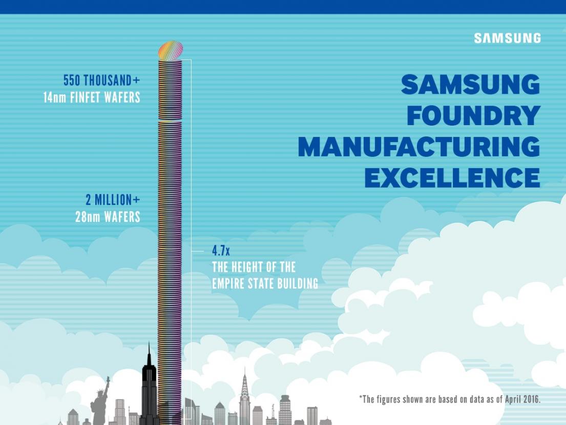
One of my favorite foundry speakers, Kelvin Low from Samsung Foundry, was on board. Let’s not forget, during Kelvin’s tenure Samsung was the first foundry to hit FinFET high volume manufacturing last year with their 14nm Exynos SoC and modem (Galaxy S6) followed by the Apple A9 SoC (iPhone 6s).
*SPOILER ALERT*
In case you are interested, Kelvin talks in detail about Samsung’s 10nm and 7nm foundry plans which are quite different from TSMC’s and GlobalFoundries’. Before Samsung, I knew Kelvin at GlobalFoundries and Chartered Semiconductor so I can tell you he is a very skilled foundry guy, absolutely.
The other guys on the panel were from Synopsys: JC Lin who spoke on Compiler II Technology Strengths for 10-nm FinFET and Andy Potemski who spoke on the 10LPE Reference Flow & ARM® Cortex®-A53 CPU Reference Implementation.
I do not know JC or Andy personally so I have included their biographies:
JC Lin
Vice President, IC Compiler II R&D, Synopsys
JC Lin has worked at Synopsys for more than 20 years. He has worked on multiple technologies and products, including logic synthesis, physical synthesis and place and route. His current focus is on the IC Compiler II place and route product. JC holds a Bachelor degree from National Taiwan University on Electrical Engineering and a Ph.D. degree from SUNY Stony Brook on Computer Science.
Andy Potemski
Senior Director, Foundry Reference Flows and Lynx Design System R&D, Synopsys Andy brings 36 years of industry experience to the table. He has been focused on design flows and automation since joining Synopsys over 21 years ago. Presently he is responsible for the Lynx Design System product R&D as well as foundry reference flow development. Prior to Synopsys, Andy spent 13 years as an IC development engineer with IBM. He holds 8 US patents in chip design and automation.


Musk’s Orbital Compute Vision: TERAFAB and the End of the Terrestrial Data Center