Each year at the International Test Conference(ITC) we hear about the latest advances from the testability side of both EDA vendors and academics. This year Aart de Geus, Chairman and Co-CEO of Synopsys delivered a keynote speech titled, “Testing Positive, for Complexity“. Yesterday I spoke with Robert Ruiz and Savita Banerjee of Synopsys by phone to glean insight into two of their new technology advances:
- Slack-based cell-aware test, inside of TetraMAX
- BIST for Embedded Flash, part of the STAR Memory System
Synospys has been offering test automation tools and IP for many years now, and along with competitor Mentor Graphics they dominate this space.
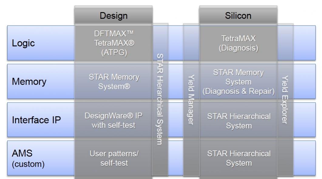
SemiWiki readers have heard much about FinFET technology on the design side, and it turns out that FinFET transistors introduce new types of silicon defects which then must be detected during test like opens in FinFET multi-finger gates. Even at the 16 nm node with the non-planar topology there are new failure mechanisms to take into account like bridging faults.
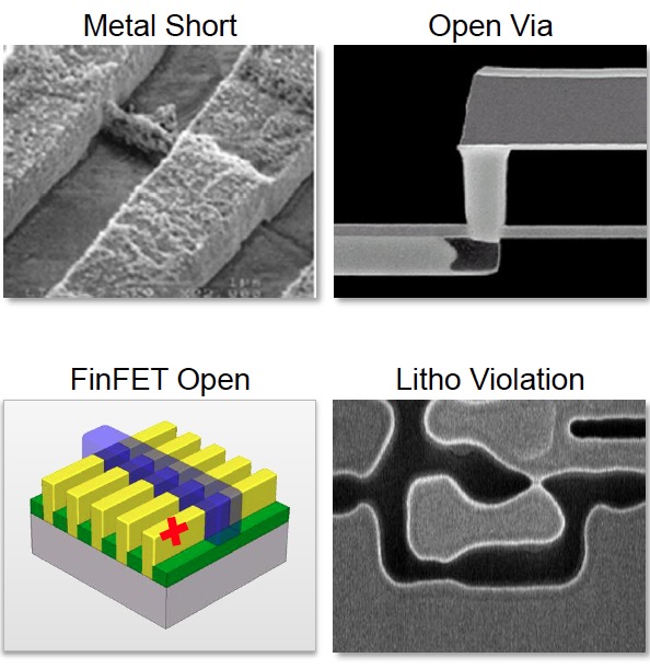
It’s no longer sufficient to assume that the only failures in an IC design are between cells, so we must be able to detect all possible defects inside of each cell too.
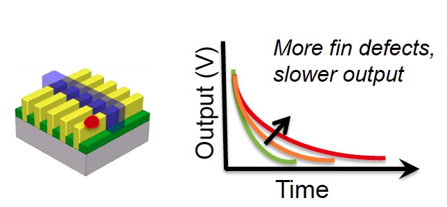
A defect on just one of the many fins in a FinFET transistor will make the output transition time slow down, but still logically function:
To address these latest test concerns Synopsys has added new technology dubbed “slack-based cell-aware test”. Defects internal to a given cell are now detected during ATPG (Automatic Test Pattern Generation) by either automatically or manually defining a sequence of vectors per cell.
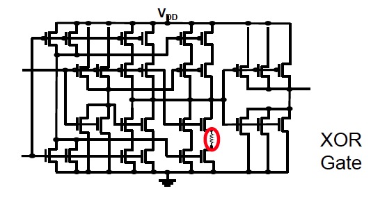
To understand slack-based test consider the following example where an XOR gate with an internal defect (marked as Red Dot) causes that cell to perform more slowly, taking an extra 30 ps to transition. The closest flip-flop to receive this slower XOR signal has a slack time of 50 ps, so the extra 30 ps delay is not detected.

There’s a second, much longer path connected to this same XOR gate, and it’s slack is only 10 ps so the 30 ps slower XOR signal will now be detected at the flip-flop in green:

An actual 28 nm TSMC customer design with this scenario was run through TetraMAX to catch and identify the fault.
Synopsys Tool Flow
If you own all Synopsys tools, then the flow to setup and run a slack-based cell-aware test includes four EDA tools:
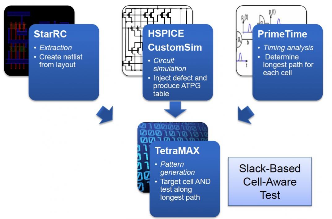
You can still use TetraMAX with other EDA vendor tools for: extraction, circuit simulation and static timing analysis. Some scripting is required.
Test Results
That customer design block in 28 nm compared cell-aware testing which found 2,347 faults, to slack-based cell-aware which found 3,323 faults, an improvement of 40% more faults detected. The number of patterns did increase from 263 to 439, or 66% to get the improved coverage, so there is increased test time involved.
Avago reported that using slack-based cell-aware test versus just slack-based improved the fault coverage inside cells from 16.4% to 67.4%, and delay faults were improved from 81% to 89.6%, all by just adding 2% more patterns.
Test Compression
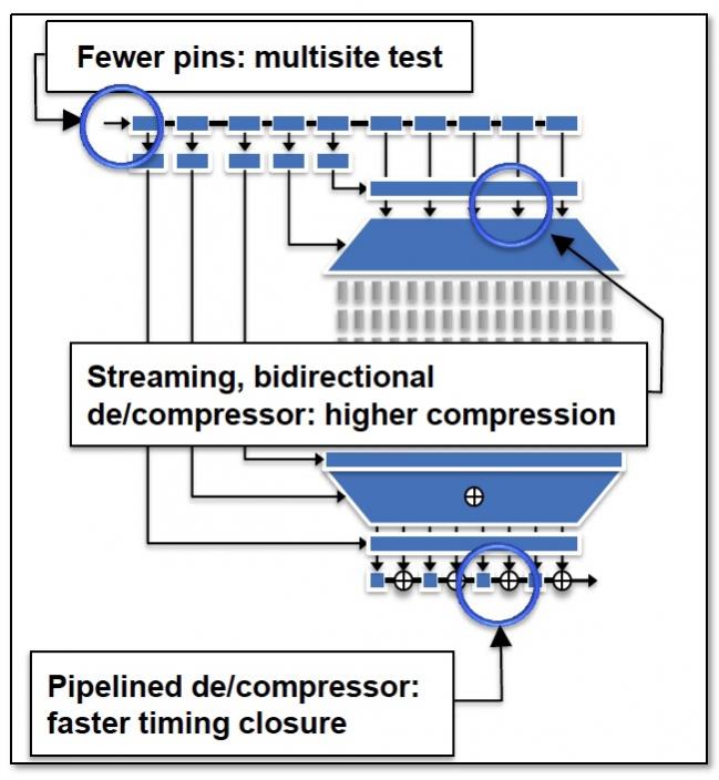
Synopsys calls their test compression approach DFTMAX Ultraand it enables higher defect coverage with lower test costs.
BIST for Embedded Flash
Next up was Savita and she introduced their new BIST technology for embedded flash, now part of the DesignWare STAR Memory System. The Flash IP is shown in green, connected to a wrapper in purple, then controlled by a test processor in purple (SMS Processor):
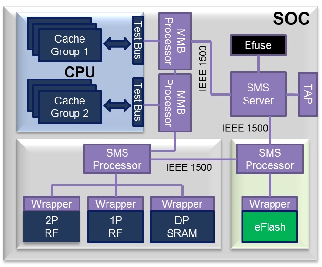
Without BIST for Flash you would have to use an expensive tester, adding time and cost to your project. Using the BIST for Flash approach you can decrease test costs by 20%, use a standard IEEE 1149.1 tester interface, and even do in-field diagnostics compliant with ISO 26262. UMC is the first foundry to support this BIST technology at their 55 nm node, so stay tuned for more foundries to become supported as well.
Summary
Test coverage is critical to ensuring that our consumer and commercial products are defect free, and the engineers at Synopsys have added new technology like slack-based cell-aware test, and BIST for embedded Flash to keep pace with market and technology demands.


Comments
There are no comments yet.
You must register or log in to view/post comments.