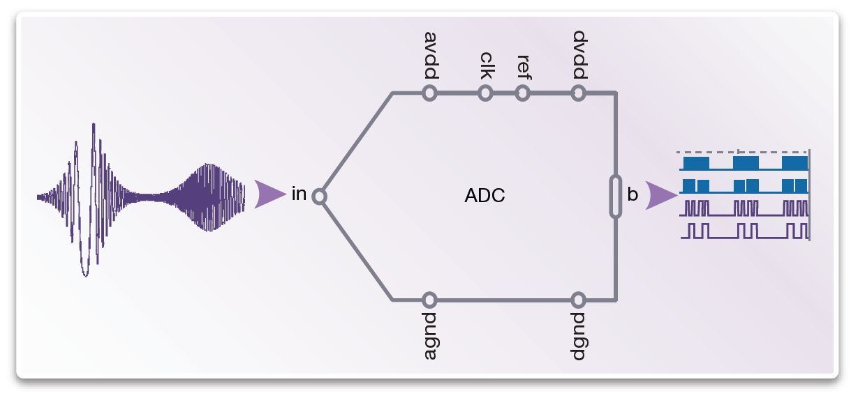
Our world is decidedly analog, made up of stimuli for our five basic senses of sight, touch, hearing, taste, and smell, and more advanced senses like balance and acceleration. To be effective on the Internet of Things, digital devices must integrate with the analog world, interfacing with sensors and control elements.
When presented with an analog interfacing requirement, some digital designers run screaming from the room. Analog and RF design have this stigma of being difficult, temperamental, and unpredictable, and in the hands of the unskilled practitioner they can be scary. Analog people also speak a funny language, talking about things like ground loops, and reference voltages, and guard bands, and signal-to-noise ratios, and galvanic isolation, and a bunch of other things digital designers may not have learned about in school.
Is it possible for a digital designer to successfully design analog interfaces into an SoC? If the task were to create circuitry from scratch, dealing with all the above variables and many more, the chances of success wouldn’t be good. Fortunately, there is help for the analog-challenged, in the form of proven IP and a checklist for integrating it into an SoC design.

A lot goes in to making analog IP blocks – such as analog-to-digital (ADC) and digital-to-analog (DAC) converters – robust for use. Voltage references usually have to be created from the digital supply rails, with resilience to switching noise from the digital logic. Analog circuits also vary with changes in voltage and temperature, and compensation must be offered. Let’s assume for a second that you have a solid, proven, process-worthy analog IP block that has been fielded in another mature design. What should you be concerned with when placing data converter IP into a new, complex SoC design?
This is where a checklist would come in really handy. Although checklists are by no means foolproof, they do capture the list of concerns where designers should focus attention and offer steps that if followed can prevent many problems. The folks at Synopsys have developed such a checklist to accompany their data converter IP offerings.
One key element of most analog designs is distance. Designers always want to minimize analog signal runs, keeping conversion circuits close to I/O pins, and when possible create separation between high-speed noisy logic and the susceptible analog IP.
Another element in analog design is the concept of differential pairs and shielding. Analog signals are usually externally referenced and isolated, providing their input in a pair of lines with signal strength corresponding to voltage difference. This provides free noise rejection provided the pairs are routed together, because noise induced on one line is induced on the other, and the net voltage difference is close to null. Sheilding can help in sensitive areas of a design, particularly where trace crossings are unavoidable and might place more noise on one of the differential analog traces.
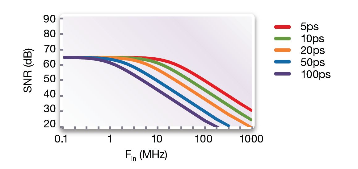
Clock jitter is a term digital designers are very familiar with, and it is also a key consideration for data converter IP. Jitter can cause a huge degradation in accuracy of analog sampling. Techniques such as short clock runs, managing slew rate, and keeping analog clocks on the same supply domain are just some of the ideas.

These and more ideas are presented in a Synopsys white paper, authored by Roberto Guerreiro and Manuel Mota:
Twelve Design Techniques for Successful Integration of Data Converter IP into an SoC
As more digital designers are finding their SoCs deployed in an analog world, this information combined with robust data converter IP can help ease many of the mysteries that appear, and increase the comfort level with analog IP nearby.
Share this post via:


Comments
0 Replies to “Integrating your SoC into the analog world”
You must register or log in to view/post comments.