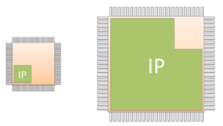
I love starting a new project from scratch, because there’s that optimistic feeling of having no constraints and being able to creatively express myself and get the job done right this time. For SoC designs today there are teams of engineers and maybe a program manager plus a marketing person that define the features, budget and most importantly the schedule. Because of time to market demands, competition and support of legacy features, we no longer have the luxury of literally starting from scratch, so semiconductor IP re-use is a firm reality. Back in the 1980s your SoC maybe had a handful of re-usable IP blocks, while today the typical SoC will be filled with a majority of IP blocks, so times have changed dramatically.
If you’re using hundreds or even thousands of IP blocks, how do you manage all of that during the design process as new versions are released, bugs are fixed, new features added, or even when the specifications change?
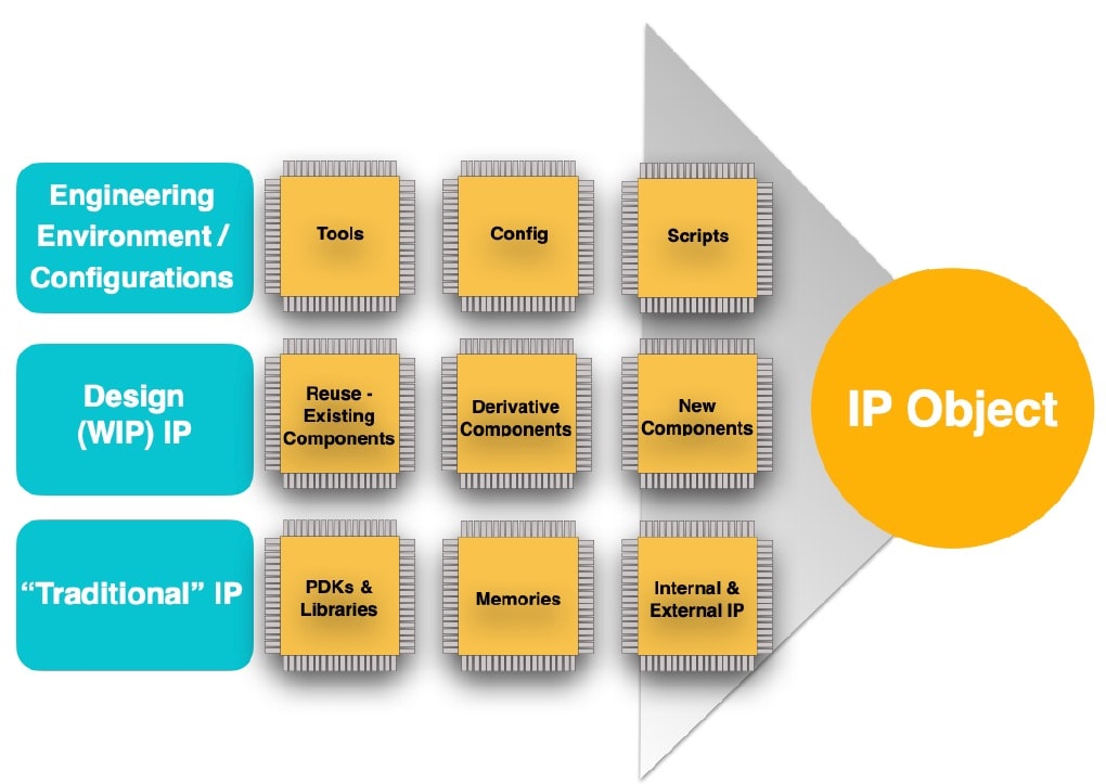
My contacts at Methodics have built their entire company around addressing this very issue, and their answer is a software tool called Percipient which is an IP Lifecycle Management Platform (IPLM). Their IP-centric approach uses hierarchy to represent your complex electronic design, and with Percipient they introduce the concept of an IP object that goes beyond just semiconductor IP:
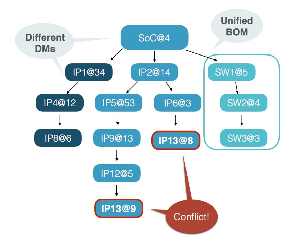
Through the use of hierarchy all dependencies of a project are tracked in one place, by design. All of the items shown above in orange are modeled as IP inside of Percipient, and every IP has dependencies defined in a hierarchical tree. The following diagram shows an SoC with versions for each IP and Software block being used, so it’s a quick way to create a Bill Of Materials (BOM):
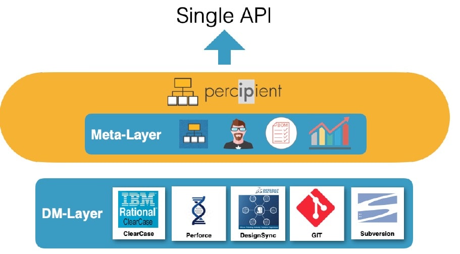
Delving a bit deeper into the electronic design process, the data for an IC is a mixture of both binary and text files, based on which EDA tool is being used, so yes, lots of different file formats and databases are used. You may have some engineers using Git or Mercurial as Data Management (DM) tools on your teams that are distributed geographically and they require close collaboration for source code development. For binary files there are other DM tools like Perforce which can handle big file sizes and be replicated across multiple sites. EDA vendor tools also tend to have their own binary file systems. With Methodics the solution was to create a DM layer that works with any tool:
Just keep using your favorite DM tools, without having to learn something new: ClearCase, Perforce, DesignSync, Git, Subversion. Percipient will work with each of these native DM systems behind the scenes, building the trees and project workspaces.
In addition to working with the most popular DM tools, there is something that Percipient provides for each IP, and that’s called meta-data which could includes things like:
- Who may view or modify an IP
- IP dependencies
- Technical specifications of an IP
- Business properties of an IP
- Conflict resolution across the hierarchy
- Workspace building rules
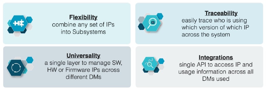
There are four benefit of using meta-data that is separate from IP data for each IP object:
With Percipient each user builds their own workspace, and each workspace is tracked, so Percipient knows which user has built each workspace, and which IP objects are in all workspaces. Team members use the familiar and native DM commands to build a workspace, so all IP stays in its original data format, along with the hierarchy.
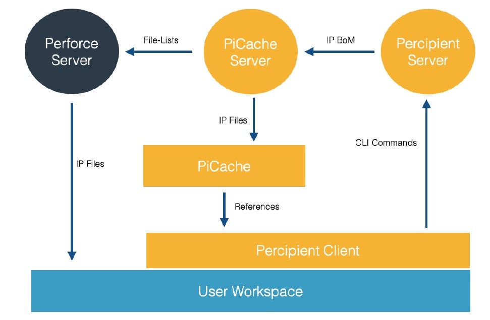
Percipient can also track all IP in the workspace as a link to a managed IP Cache, which is also called PiCache. With this concept each IP version is saved for use by any workspace through soft-links. Here’s a diagram of how IP Cache operates:
A big advantage of using IP Cache is that a workspace can be built literally in just seconds, and it uses very little space because links are used to the cache. An engineer could choose to make an IP object “Local” through check out with the DM tool, or keep them as links. You make an IP local when making modifications, otherwise leave it as a soft link.
Summary
The vast complexity of a modern SoC calls for fresh thinking on an efficient design methodology, and with the proliferation of semiconductor IP re-use it makes sense to have a methodology that is IP object centric. Methodics have done a foundational work in this area of IP Lifecycle Management, and their Percipient tool has been integrated with the most popular Data Management tools in the industry, so you don’t have to ask the CAD department to make your tool flow work with custom programming.
Read the complete 10 page White Paper online now.
For chip design teams in Taiwan and China, there’s some good news as Methodics has recently added a new sales representatives in each country. It’s great to live in the same time zone as your customers.
Related Blogs
- SEMI Takes the Jim Hogan and Simon Butler Conversation Virtual
- Project-centric Design Process, or IP-centric
- Avoiding Fines for Semiconductor IP Leakage
- UPDATE: Everybody Loves a Winner




Comments
There are no comments yet.
You must register or log in to view/post comments.