You are currently viewing SemiWiki as a guest which gives you limited access to the site. To view blog comments and experience other SemiWiki features you must be a registered member. Registration is fast, simple, and absolutely free so please,
join our community today!
The recent Chiplet Summit at the Santa Clara Convention Center was buzzing with many enabling technologies for chiplet-based design. Collaboration was also on display during many parts of the show. A presentation in the Siemens booth was a perfect example of both of those trends. In the Siemens booth, Perforce presented an excellent… Read More
GenAI is certainly changing the world. Every day there are new innovations in the use of highly trained models to do things that seemed impossible just a short while ago. As GenAI models take on more tasks that used to be the work of humans, there is always a nagging concern about accuracy and bias. Was the data used to train the model … Read More
On July 9, 2025, Michael Munsey, VP of Semiconductor Industry at Siemens, and Vishal Moondhra, VP of Solutions at Perforce, presented a DACtv session announcing their strategic partnership, as seen in the YouTube video. This collaboration integrates Siemens’ digital twin and digital thread technologies with Perforce’s version… Read More
As the new name reflects, chip and system design were a major focus at DAC. So was the role of AI to enable those activities. But getting an AI-enabled design flow to work effectively across chip, subsystem and system-level design presents many significant challenges. One important one is effectively managing the vast amount of… Read More
AI technology was prevalent at DAC 2025, but can we really trust what Generative AI (GenAI) is producing? Vishal Moondhra, VP of Solutions Engineering from Perforce talked about this topic in the Exhibitor Forum on Monday, so I got a front row seat to learn more.
Vishal started out by introducing the four challenges and risks of using… Read More
Stop by the Perforce booth to learn about our new partnership with Siemens and get a demo of the latest enhancements in Perforce IPLM, P4, and VersIC. We’re eager to hear about your current challenges and how our semiconductor design and data management solutions can ease your design and development hurdles. Plus, you can try your… Read More
In this inaugural episode of the new Semiconductor Insiders video series, Dan is joined by Vishal Moondhra, VP of Solutions Engineering at Perforce Helix IPLM. Dan explores the risks and challenges of using Gen AI in the semiconductor industry with Vishal. Liability, traceability, cost, and quality are discussed. The challenges… Read More
Perforce powers innovation at unrivaled scale. Perforce solutions future-proof competitive advantage by driving quality, security, compliance, collaboration, and speed – across the technology lifecycle. We bring deep domain and vertical expertise to every customer, so nothing stands in the way of success. Our global footprint… Read More
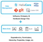
Most large electronics companies take a divide and conquer approach to projects, with clear division lines set between HW and SW engineers, so quite often the separate teams have distinct methodologies and ways to design, document, communicate and save a BoM. This division can lead to errors in the system development process,… Read More
Back in July I first read the news that Perforce had acquired Methodics, and wasn’t too surprised, because many of the EDA vendors that we blog about do get acquired or merge with similar sized companies in order to be part of a bigger offering. When Methodics announced a webinar introducing IPLM 3.0 (IP Lifecycle Management),… Read More