If the thought of a silicon respin keeps you awake at night, you’re not alone. Re-fabricating a chip can cost tens of millions of dollars. An unplanned respin also risks a delay in getting a product to market, which adds tremendous costs in terms of lost business.
Undoubtedly, adding to your sleep loss is the recent rise in respins. What’s causing this increase of failures when the design gets to silicon? As electronics products add increasing numbers of features and faster performance, things have gotten complicated. A patchwork of silicon IP, 100s of millions or billions of transistors, and the challenge of getting analog and digital to play in the same sandbox, has resulted in Byzantine sprawls across the die. Meanwhile, the growth of electronic components needed in AI solutions, automotive, 5G connectivity, gaming, medical IoT, and more continues to mushroom. For instance, contrast the abundance of electronics in today’s self-driving cars with your uncle’s Buick.
Complexity gone wild
As they race to satisfy this demand, companies are trying to fit all circuitry on the same substrate or on a single technology node. The latest process technologies plus cost-effective innovations in transistors, such as gate-all-around (GAA), further enable engineers to pack previously unfathomable numbers of transistors onto a die. Apple’s ARM-based dual-die M2 Ultra SoC, which is fabricated using TSMC’s 5 nm semiconductor manufacturing process, packs 134 billion transistors. And TSMC is charting a course for manufacturing one-trillion-transistor chips in 1nm.
This kind of complexity can cause everything from power issues to analog circuitry failing or falling out of operable range. And chipmakers are pushing into smaller and smaller nodes, which creates more challenges to success in manufacturing. For example, “The data suggest smaller node size and larger gate count are a contributing factor to power-related respins,” according to a recent article on Siliconengineering.com. “That means power could be the number one cause of respins for the biggest designs at the latest nodes, and that is before adding in the failures that are not recorded as ‘power-related’.”
Compounding the challenges of finding and fixing bugs or functional defects early in a design is the shortage of experienced designers. Complex SoC is a complex endeavor, which requires, for example, the ability to interpret design intentions from the schematics and understand arcane topics like transistor matching, noise tolerance, and parasitics.
Advanced device modeling to the rescue
So, how can you get your sleep back and avoid costly respins? Join a comprehensive webinar focused on enhancing device reliability and preventing silicon respins through innovative noise and binning modeling technologies. Keysight Technology engineers will give you deep dives into two combinations of tools and techniques that will reduce your chances of a chip failing in silicon.

The first speaker covers enhancing reliability with accurate noise measurement and modeling. Precise noise data in device modeling is critical to design and manufacturing success. In the massively complex devices we just described, accurately accounting for noise is essential for ensuring reliability. You will learn how noise data across the wafer can serve as an early indicator of device performance, particularly in low-signal applications such as communications circuits, quantum computing, and image processing. Keysight will walk you through using the company’s Advanced Low-Frequency Noise Analysis (ALFNA). And you will get a first-hand look at how easy it is to use the system to measure and analyze 1/f and Random Telegraph Noise from DC to 100MHz, enabling you to refine designs and boost overall reliability. Key takeaways include:
- The impact of precise noise modeling on device reliability and performance
- How Keysight’s ALFNA system can improve noise data integration and analysis

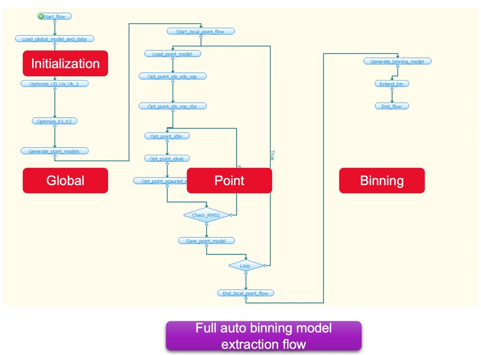
Next, you’ll learn how to streamline your device modeling workflow to help you avoid respins with automated binning model extraction. As devices become smaller and more complex, traditional global models often fall short in accuracy. You’ll see how binning models offer improved precision—which is critical to the success of your complex designs—and how you can streamline the difficult and time-consuming process of developing them. A Keysight engineer will conduct a live demonstration of an automated extraction flow that enhances binning model efficiency. This will include showing you how Keysight automation techniques and fast QA methods simplify and accelerate the binning process. Key takeaways include:
- Techniques for automating binning model extraction to avoid costly respins and enhance modeling efficiency
- Strategies to streamline the QA process and accelerate model development
So, if rising device complexity and shrinking process nodes make you anxious about functional flaws or bugs getting away and causing re-spins, this webinar will hopefully lower your stress levels. The advanced device modeling tools and techniques covered by Keysight experts are not only easy-to-use but can also significantly improve device reliability and prevent costly design errors.
To see the replay, visit Maximize Reliability and Yield with Advanced Noise and Binning Modeling.
Read: Seeing 1/f noise more accurately
Also Read:
Keysight EDA and Engineering Lifecycle Management at #61DAC
PCIe design workflow debuts simulation-driven virtual compliance
Keysight EDA at the 2024 Design Automation Conference
Share this post via:


Comments
There are no comments yet.
You must register or log in to view/post comments.