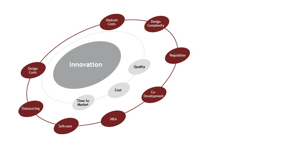
During my long career in semiconductor, EDA, I have heard, believed and experienced that this is a knowledge industry swamped with rapid innovation and technology drivers; typical manufacturing product development processes like Gantt charts and others do not apply here. The fallback is that most of the time estimations are ad hoc, based on gut-feel or expert opinion. Not only schedule, most of the processes are run by individual preferences; in other words the whole process is more people driven than process driven. Naturally, we see missed targets, re-spins, cost overruns, lost market opportunities and so on. It is said that success rate to first silicon is 0%! And we attribute the Product Lifecycle Management (PLM) issues to high complexity of designs at nanometer scale, high density, analog and digital mixed-signal and so on.
After I read the Kalypso white paper on Semiconductor Lifecycle Management at Dassault website located at –
Semiconductor Product Lifecycle Management Industry Adoption, Benefits and The Road Ahead
my perspective changed. Yes, I believe if we take PLM as a strategic direction towards improving product lifecycle in semiconductor space, many of the issues related to short window of opportunity, time-to-market, reduced design cost, profitability etc. can see significant improvement.
So where is the problem? Why is PLM adoption slow in Semiconductor space? As I have experienced myself, there is no common standard packaged PLM tool in this space, amplified by lack of awareness and limited understanding of value proposition of PLM. It is important that a product must be looked at not only from technical angle, but also from commercial angle.
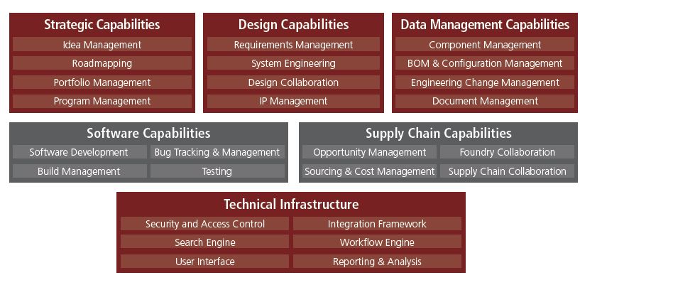
[Components of a comprehensive PLM solution for Semiconductor industry]
The white paper describes in great detail the analysis by Kalypso researchers (who interviewed Semiconductor industry executives) and proposes a comprehensive method of PLM specifically for Semiconductor industry which includes complete value chain including design, software, data management, supply chain and so on. A key message here is “Think big, start small, move fast and build incrementally”. By using this principle the PLM strategy can be successfully implemented. Unless it is fully implemented, we do not see major results. Often we try to do it all at once and end up with dissatisfaction. If implemented gradually and completely, I am sure we then start seeing results project after project.

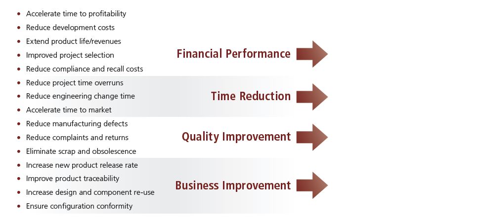
With strategic PLM program in place companies are seeing time-to-market and time-to-profit being condensed by 5 to 30% meaning more revenues due to improved market penetration. It also frees up R&D resources to work on other new product development early in the cycle. Also, PLM helps in commercializing and launching products globally and concurrently. A summary of PLM benefits is concisely listed as –
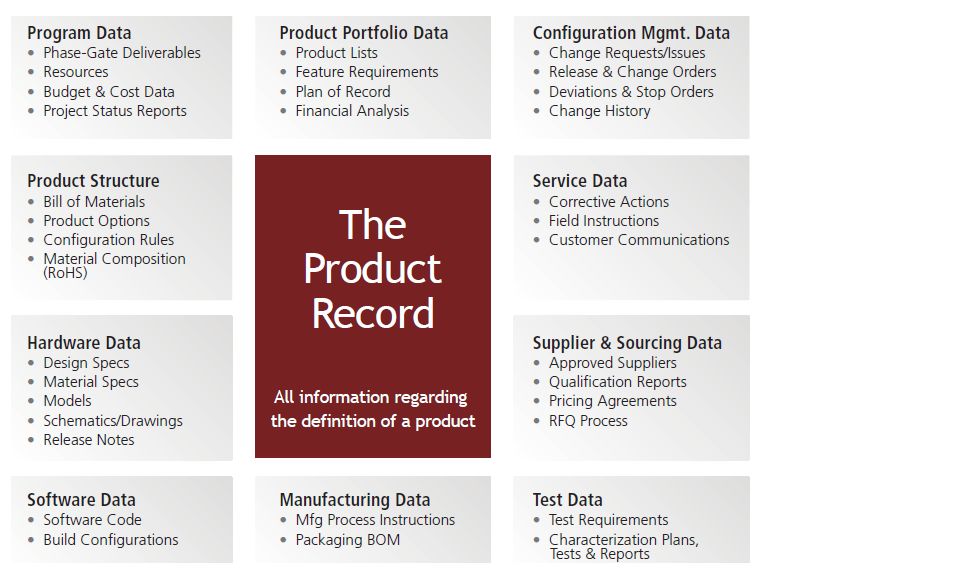
PLM provides a single comprehensive repository of complete data about any project which includes overall value chain. Once implemented this provides great ease in re-use, process improvement and implementation of subsequent projects.
Some of the early adopters have seen the benefits of PLM in semiconductor space. A long term strategy needs to be built starting with a high impact business problem and then building on it to realize the full potential of the system for the overall business.
Share this post via:


Musk’s Orbital Compute Vision: TERAFAB and the End of the Terrestrial Data Center