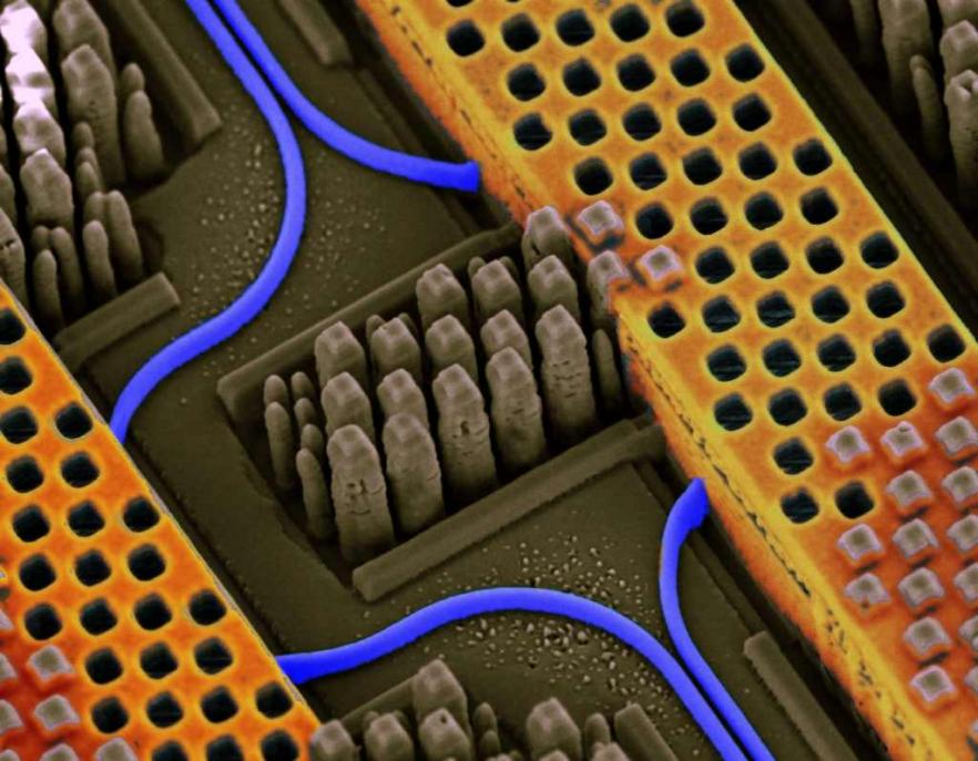
Silicon Photonics is the hottest prospect for blazing fast communication between chips in servers, data centers, and supercomputers.

By using light instead of electrical signals, it promise to usher in a new standard of high performance, low power devices while extending the use of more mature process nodes, helping to reduce overall costs. Of course, nothing comes completely free. While it may be possible to utilize the same fabs and manufacturing techniques, as demonstrated recently by IBM (SPIE 2015), the design and testing of photonic devices is quite different than that of the traditional IC. Learning how to design silicon photonic circuits takes some effort, and doing it on your own is a tough task.

Fortunately, there is now an online course, which starts on 7 July, 2015,available through edX that can give you hands-on practice in the design of photonic circuits. Under the instruction of Professor Lukas Chrostowski, a leader in the field, you will actually step through the entire process of design creation, simulation, and verification of a silicon photonic circuit. For this course, Mentor Graphics is providing students with access to the Pyxis IC layout tool and the Calibre physical verification tools required to create and verify photonic circuit designs using a secure remote cloud infrastructure.
 This 6-week course allows you to create, edit, and upload real design data. The upload calls Mentor Graphics’ Calibre tools to perform error checking (for compliance to manufacturing constraints and design testability requirements), and performs mask aggregation and generation of automated test vectors. It also enables students to perform peer design reviews and provide feedback on each other’s designs.
When completed, the student designs will be collected and actually manufactured! The manufactured circuits will then be tested using a novel photonic test bench approach. While you won’t have access to the final manufactured chip, you will receive the results of the post-manufacture test results for analysis and validation of their design approach.
Ultimately, this training could help you dramatically cut your learning curve and shorten the leap to the rewards of silicon photonics design. Interested? Get more information and register for the course here.
Share this post via:


Comments
0 Replies to “How to design silicon photonics–take this class!”
You must register or log in to view/post comments.