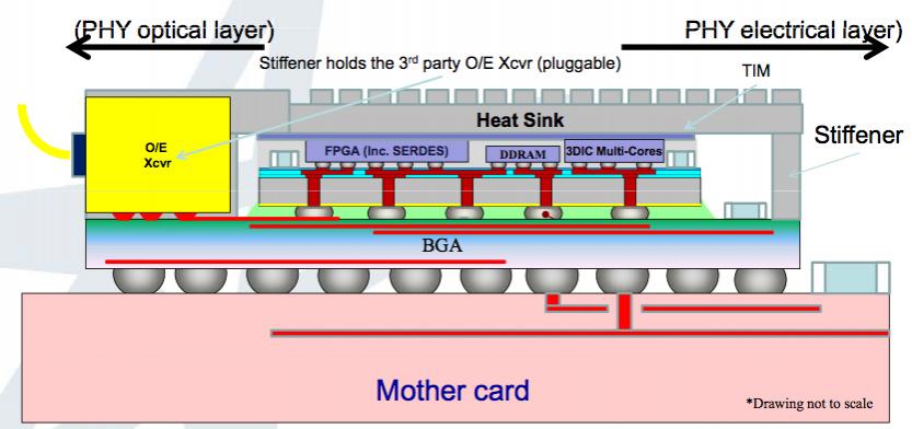
I attended the 3D architectures for semiconductor integration and packaging conference just before Christmas. I learned a lot and have put together an overview of what is going on in 3D ICs. This is not intended for experts (and if I’ve made egregious errors then please correct them in the forum) but more for people who are not doing 3D designs and are wondering how this might impact them in the future. All in the new 3D ICs forum. The overview is in two parts because it is so long.
lang: en_US
Share this post via:


Silicon Insurance: Why eFPGA is Cheaper Than a Respin — and Why It Matters in the Intel 18A Era