There is always a rush to converge a semiconductor design toward faster closure, amid increasing divergent trends of multiple IPs and high complexities of various functionalities on a single chip. Every design house struggles hard to evolve its customized design flows with several short paths patched up to fix issues, global or local, at each stage in the design flow. And that becomes severe at the final layout stage, acting like a point of no return and warns – fix what you can, here and now, otherwise you are bound to lose the market window. Often one needs to compromise in terms of area and/or performance. Not a pleasant situation!
I wanted to understand how SpyGlass deals with layout situations early at RTL. What I found is this – start at RTL with the layout in mind! I was delighted to have an opportunity talking to Sanjiv Mathur, Sr. Director atAtrenta’s Noida site. I know Sanjiv since my Cadence days when he was in my Physical Design team. He used to provide innovative ideas in the physical design domain, so my guess was right, he is part of a team which has done something really great in SpyGlass Physical. Here is our talk:
Q: Sanjiv, you have been associated with multiple facets of SpyGlass Physical, what are those you are currently working with?
SpyGlass Physical Base functionality concentrates on structural aspect of the design and works at RTL to determine a design construction which can lead to an optimal distribution at the layout level thus reducing long iterations. It takes into account various rules at the pre-floorplan level, satisfies those, and then provides RTL signoff to post-floorplan processes.
Q: What are the pre-floorplan rule checks?
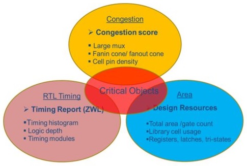
These rules are majorly classified into congestion, timing, and area rules and there are critical structures that violate most of these rules. Critical structures need special attention to make them free from those issues. If large size of a mux, high fan-in and fan-out cones at FFs, high cell-pin density in a module, etc. can cause congestion, then they can easily be detected at RTL through the use of some rules. Similarly, long depth of logic level can lead to timing violations. So, there are specific rules used to capture these issues at RTL, which are then resolved by employing special techniques. For example, pipelining is used to reduce high fan-out cone and splitting is used to reduce high fan-in cone.

[Physical rules employed at RTL]
Q: Do physical rules follow any standard language for their description?
No, these are SpyGlass specific, built into the tool. Any designer can enter them through graphic entry or they can write them as text into a project file (prj file) which has all kinds of descriptions such as HDL (Hardware Description Language), SDC (Standard Design Constraint), technology information and the rules. For analyzing these rules, cross-probing between RTL and schematic is provided.
Q: This looks like a novel idea to resolve issues at RTL. What is your experience on the kind of change in the design that takes place after RTL handoff?
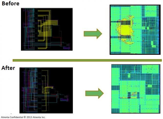
Yes, we have a patent pending on this unique way of estimating congestion based on RTL structures. The change in design is quite appreciable. Below is an example of a real design before and after RTL modification.

Q: Great!! These rules and methods seem to be good to detect and resolve gross structural violations. What do you do when issues come after RTL handoff?
Yes, that is where SpyGlass Physical Advanced comes into the picture which provides handoff quality design by signing off post-floorplan metrics. In an SoC design flow (which can have multiple complex IPs and hard macros along with other design elements), it does partitioning and data flow analysis, divides the design into multiple physical units (PUs), partitions the bus fabric to cater to each PU such that there are minimum logic and clock crossings and there is timing closure. By employing floorplanning, StdCell placement and global routing, it can provide physical congestion scores, thus optimizing the area and satisfying timing closure. It also provides physical guidance to improve efficiency of downstream implementation tools, such as channel planning and estimation.
Q: O.K. that’s a good differentiation between Base and Advanced. How do you make them as separate offering?
It’s the best combination to use SpyGlass Physical BaseandAdvanced together which can provide an optimized floorplan in the form of DEF (Design Exchange Format) or physical constraints. However, for small designs they can use just SpyGlass Physical BaseforRTL signoff and then do the rest of physical implementation on their own. For SoC and complex IP designs, SpyGlass Physical Advanced is the ultimate choice since predicting design closure before entering implementation flow is becoming essential with shrinking technology nodes. It makes the downstream flow smoother by reducing iterations and optimizing on performance and area.
Q: SpyGlass Physical appears to be a great set of tools, who all are using it?
It’s integrated into TSMC IP Kit 2.0. Major design and IP companies and foundries in US, Europe and Japan are using SpyGlass Physical.
It was a great eye opener session with Sanjiv. It reminded me about two of my patents in my earlier job, about five years ago, which, at that time, tried to predict layout congestion at the floorplanning stage based on the block placement and pin assignment in the floorplan. However, that didn’t have a much broader and global context as seen from the RTL level and also there was no pre-floorplan consideration. SpyGlass approach is much superior which starts design refinement to reduce layout congestion right from the beginning at RTL level.

More Articles by Pawan Fangaria…..
lang: en_US
Share this post via:


Silicon Insurance: Why eFPGA is Cheaper Than a Respin — and Why It Matters in the Intel 18A Era