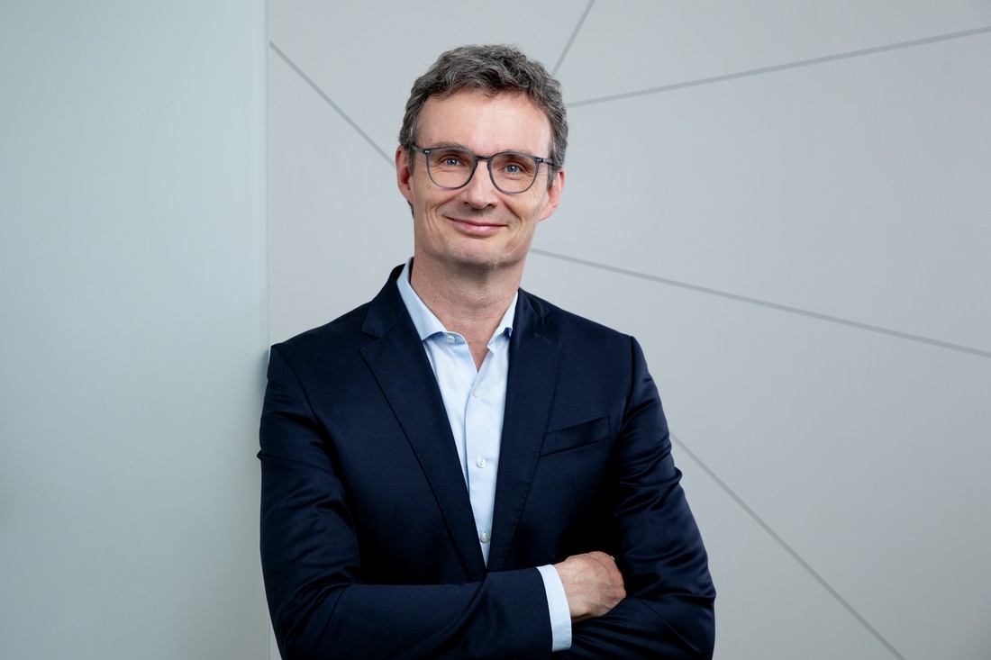
With over 25 years of experience in the specialty materials industry, Dr. Heinz Kaiser is a member of the Management Board of SCHOTT AG, responsible for High-Performance Materials and Flat Glass, while also heading Sales and Market Development, Sales Excellence, and Intellectual Property. With a strong engineering background and extensive international leadership experience, he brings a strategic, innovative perspective to advancing SCHOTT’s technology businesses in demanding global markets. Throughout his career, Dr. Kaiser has held senior roles across operations, strategy, and global business management, giving him a deep understanding of complex manufacturing environments and long-term value creation. He is widely recognized for combining technical excellence with strategic clarity to drive sustainable growth and innovation.
Tell us about your company?
SCHOTT is an international technology group that produces high-quality components and advanced materials, including specialty glass, glass-ceramics, but also polymers. With over 140 years of experience, our expertise spans the entire value chain from raw material production to precision-engineered components, ensuring quality, scalability, and reliability for our partners worldwide. For over two decades, SCHOTT has supplied essential materials and solutions for chip manufacturing, packaging, and lithography, supporting the world’s leading equipment manufacturers, foundries and integrated device manufacturers (IDMs). Our expertise in glass core panels, carrier wafers, and ultra-pure quartz glass helps drive the next generation of high-performance, energy-efficient semiconductors. For over two decades, SCHOTT has supplied essential materials and solutions for chip manufacturing, packaging, and lithography, supporting the world’s leading equipment manufacturers, foundries and integrated device manufacturers (IDMs).
What problems are you solving?
SCHOTT’s engineered glass solutions help to support advanced lithography, device fabrication, and advanced packaging processes in the semiconductor manufacturing supply chain. As traditional transistor miniaturization approaches physical boundaries, SCHOTT’s advanced glass substrates and packaging solutions enable continued progress in chip performance and miniaturization.
What application areas are your strongest?
- Chip Fabrication: SCHOTT manufactures highly precise carrier wafers and, recently, carrier panels, to support processes such as wafer thinning, back grinding, and fan out packaging.
- Chip Packaging: SCHOTT manufactures glass panels for use in glass core substrates. Glass provides a significant advantage over existing materials in terms of stiffness, surface roughness, electrical properties, variable CTE capability, and highly precise structurability enabling the fabrication of large size glass core substrates for packaging high performance computing systems.
- Lithography: We supply specialty glass and glass-ceramics (e.g., ZERODUR ® ) for precise positioning and stability in lithography machines, essential for chip fabrication. In addition, SCHOTT manufactures precision light guides and optics for use in the leading edge EUV lithography equipment.
- Wafer Manufacturing: SCHOTT manufactures ultra-pure quartz glass components for use in wafer production equipment such as etch units with high stability, low thermal expansion, and excellent chemical resistance.
What keeps your customers up at night?
Semiconductor packaging design is becoming an increasingly important topic to address computational scaling demands. As such, package designers are looking into new materials to enable large area, highly dense, heterogeneously integrated systems.
The current major challenges that our customers are facing are establishing reliable designs and scaling the manufacturing of these advanced packages. To meet performance and reliability requirements, our customers need committed material supply chain partners willing to invest in innovation. They need new glass materials, rapid sampling to support prototyping, and formal partnership to maintain ongoing support. In addition, they need secure access to these advanced materials globally at quality and precision levels consistent with semiconductor manufacturing standards.
What does the competitive landscape look like and how do you differentiate?
The semiconductor materials market is highly competitive and innovation-driven. In the world of glass, there are a limited number of highly-capable global suppliers. SCHOTT stands out by leveraging over 140 years of glass manufacturing expertise and over 20 years of support to the semiconductor industry, focusing on glass innovations to enable the development of next generation lithography, wafer manufacturing, and packaging technologies, and consistently investing in new material and process development to support these markets. We continue the expansion of capabilities through internal investment in R&D and manufacturing as well as through acquisition, including the recent acquisition of QSIL’s Quartz Glass division, and apply deep application expertise through global Application Engineering teams that support customer implementation of these developments.
What new features/technology are you working on?
SCHOTT is currently working on developing technologies to further support the commercialization of glass core substrates. This includes development of new glass compositions, process development to advance structuring capabilities, and manufacturing technologies to provide semiconductor quality panels at scale. We are also looking at adjacencies in co-packaged optics and glass interposers, both from a material and processing perspective, where glass can provide an advantage.
In the realm of carrier wafers and panels, we are working to advance dimensional tolerance capabilities beyond what exists today as well as develop new compositions with a wider range of properties including CTE, modulus, and optical transparency.
Finally, we are working with partners to develop the next generations of glass consumables, optics, light guides, and device stages to support advanced node equipment manufacturing innovation.
How do customers normally engage with your company?
Customers normally engage with SCHOTT through direct supply agreements that leverage the company’s global manufacturing and logistics capabilities for reliable delivery of specialty materials, as well as through collaborative development efforts that involve co-innovating on custom glass and ceramic solutions for specific semiconductor applications.
Engagement also includes technical support, with customers accessing SCHOTT’s expertise in materials science and engineering for process optimization, and long-term partnerships that build strategic relationships to drive innovation and meet evolving industry needs.
Also Read:
CEO Interview with Moshe Tanach of NeuReality
2026 Outlook with Paul Neil of Mach42
CEO Interview with Scott Bibaud of Atomera
Share this post via:


Chemical Origins of Environmental Modifications to MOR Lithographic Chemistry