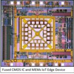
In my 34 years in IC and EDA, it never ceases to amaze me as to how ingenious designers can be with what is given them. Mentor, a Siemens business, has released a wonderful white paper that is proof of this yet again. The white paper steps through how one of their customers, MEMSIC, used the Tanner tool suite to develop a combination CMOS… Read More
CEO Interview: Michel Villemain of Presto Engineering, Inc.
One of the many advantages of being part of SemiWiki is the interesting people we get to meet. As I have mentioned before, the semiconductor industry is home to many brilliant and successful people and Dr. Michel Villemain is certainly one of them. Michel is the founder and CEO of Presto Engineering and it is interesting to note that… Read More
Getting More Productive Coding with SystemVerilog
HDL languages are a matter of engineering personal preference and often corporate policy dictates which language you should be using on your next SoC design. In the early days we used our favorite text-based editor like Vi or Emacs, my choice was Vi. The problem with these text-based editors of course is that they really don’t… Read More
Semiconductor Reliability and Product Qualification
This week, we are continuing our discussion of various topics that Semitracks addresses in their training activities. One area that they focus on quite a bit is Semiconductor Reliability and Product Qualification.
One of the key activities that a Product Engineer will coordinate is the qualification of new products before they… Read More
Making Sensors of the World
How many sensors do you think you own? Let’s start with your thermostat. It’s simple, right? You might guess one or two, and if you owned a 2[SUP]nd[/SUP] generation Nest you’d be wrong. It comes with a light sensor, heat sensor (in addition to temp), microphone, carbon monoxide sensor, smoke sensor, and occupancy sensor. Also, … Read More
CEO Interview: Jim Gobes of Intrinsix
Experience gives us the ability to make better decisions and in a fast moving industry like semiconductors, experience is critical. As chips get more integrated and complex the number of design decisions that must be made increases at a dramatic rate. Process technologies for example, never in the history of semiconductors have… Read More
Introduction to Semiconductor Processing
We introduced you to Semitracks last week with an interview of their CEO, Chris Henderson. This week, we thought it might be worthwhile to continue that introduction with an overview of one of their more popular online and in-houses courses:
Introduction to Semiconductor Processing.
One of the big challenges in our industry for… Read More
Is an ASIC Right for Your Next IoT Product?
According to a recent study by ARM, more than one trillion IoT devices will be built between 2017 and 2035. Based on research for an upcoming book on IoT devices and looking at SemiWiki IoT analytics I find that number to be reasonable, in fact, easily attainable. Even more interesting, the market for IoT devices and related services… Read More
CEO Interview: Chris Henderson of Semitracks
In looking at the SemiWiki analytics over the last six years it is clear that the average age of our readers is trending down. (Yes, Google knows how old we are). The 25-35 age group now represents our largest readership and that is supported by the conferences I have attended recently. At the Design Automation Conference last month… Read More
Seeking Autonomy
I’d wager that if I mention autonomous vehicles, the first thing that you would think of would be autonomous cars. The truth is that we will see many other kinds autonomous vehicles in the years ahead. Their applications will range from package delivery to saving lives on the battlefield. Of course, to some extent they are already… Read More


