You are currently viewing SemiWiki as a guest which gives you limited access to the site. To view blog comments and experience other SemiWiki features you must be a registered member. Registration is fast, simple, and absolutely free so please,
join our community today!
WP_Term Object
(
    [term_id] => 157
    [name] => EDA
    [slug] => eda
    [term_group] => 0
    [term_taxonomy_id] => 157
    [taxonomy] => category
    [description] => Electronic Design Automation
    [parent] => 0
    [count] => 4439
    [filter] => raw
    [cat_ID] => 157
    [category_count] => 4439
    [category_description] => Electronic Design Automation
    [cat_name] => EDA
    [category_nicename] => eda
    [category_parent] => 0
    [is_post] =>
)
Every year EDA vendor MunEDA hosts a user group meeting where engineers present how they used automation tools to improve their IC designs, and one presentation from Peter Huber of Infineon caught my attention, it was all about SRAM design optimization. Peter has authored papers at IEEE conferences and been issued patents related… Read More
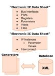
Design re-use has enabled IC design teams to create billion-transistor designs where hundreds of IP blocks are pre-built from internal or external sources. Keeping track of where each of these IP blocks came from, what their version status is, managing IP, or even discerning their license status can be a full-time job if tracked… Read More
Dan is joined by Dr. Walden Rhines. Wally is a lot of things, CEO of Cornami, board member, advisor to many and friend to all. For this discussion he is the Executive Sponsor of the SEMI Electronic Design Market Data report.
Dan explores the Q2 results summarized in the report with Wally. Overall growth was around 5%, a much lower number… Read More
Electrical copper interconnects, once the backbone of data center networks, are facing growing challenges. Rapid expansion of AI and ML applications is driving a significant increase in cluster sizes within data centers, resulting in substantial demands for faster I/O capabilities. While the surge in I/O requirements is … Read More
Dan is joined by Anand Thiruvengadam, director of product and business management and head of the Solutions and Go-to-Market functions for the memory market segment at Synopsys.
Anand discusses the substantial demands experienced by memory designers due to trends such as big data analytics. He describes how these demands impact… Read More
If you have anything to do with the semiconductor industry, you already know that one of the hottest areas for both manufacturing and EDA are systems designed with advanced packaging, basically putting more than one die (aka chiplets) in the same package.
When 3D packaging was first introduced, there were not really any effective… Read More
Semiconductor IP design re-use has enabled the relentless growth in complexity of SoC and chiplet-based systems over the years, and with IP reuse comes many unique challenges. Fabless design companies use IP provided by a vibrant ecosystem of IP suppliers and foundries, plus internal re-use in the quest to get to market more … Read More
Unreachability (UNR) analysis, finding and definitively proving that certain states in a design cannot possibly be covered in testing, should be a wildly popular component in all verification plans. When the coverage needle stubbornly refuses to move, where should you focus testing creativity while avoiding provably untestable… Read More
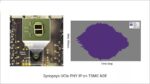
TSMC has been offering foundry services since 1987, and their first 3nm node was called N3 and debuted in 2022; now they have an enhanced 3nm node dubbed N3E that has launched. Every new node then requires IP that is carefully designed, characterized and validated in silicon to ensure that the IP specifications are being met and … Read More
Synopsys recently hosted a cross-industry panel on the state of multi-die systems which I found interesting not least for its relevance to the rapid acceleration in AI-centric hardware. More on that below. Panelists, all with significant roles in multi-die systems, were Shekhar Kapoor (Senior Director of Product Management,… Read More


Chemical Origins of Environmental Modifications to MOR Lithographic Chemistry